Hi!
Years ago ( 🙁 ) I wrote an article with the purpose of starting a series to introduce various IoT concepts to hackers and penetration testers that approach the topic for the first time. Unfortunately, that article was left alone for a long time, but now it’s time to continue that series of posts!
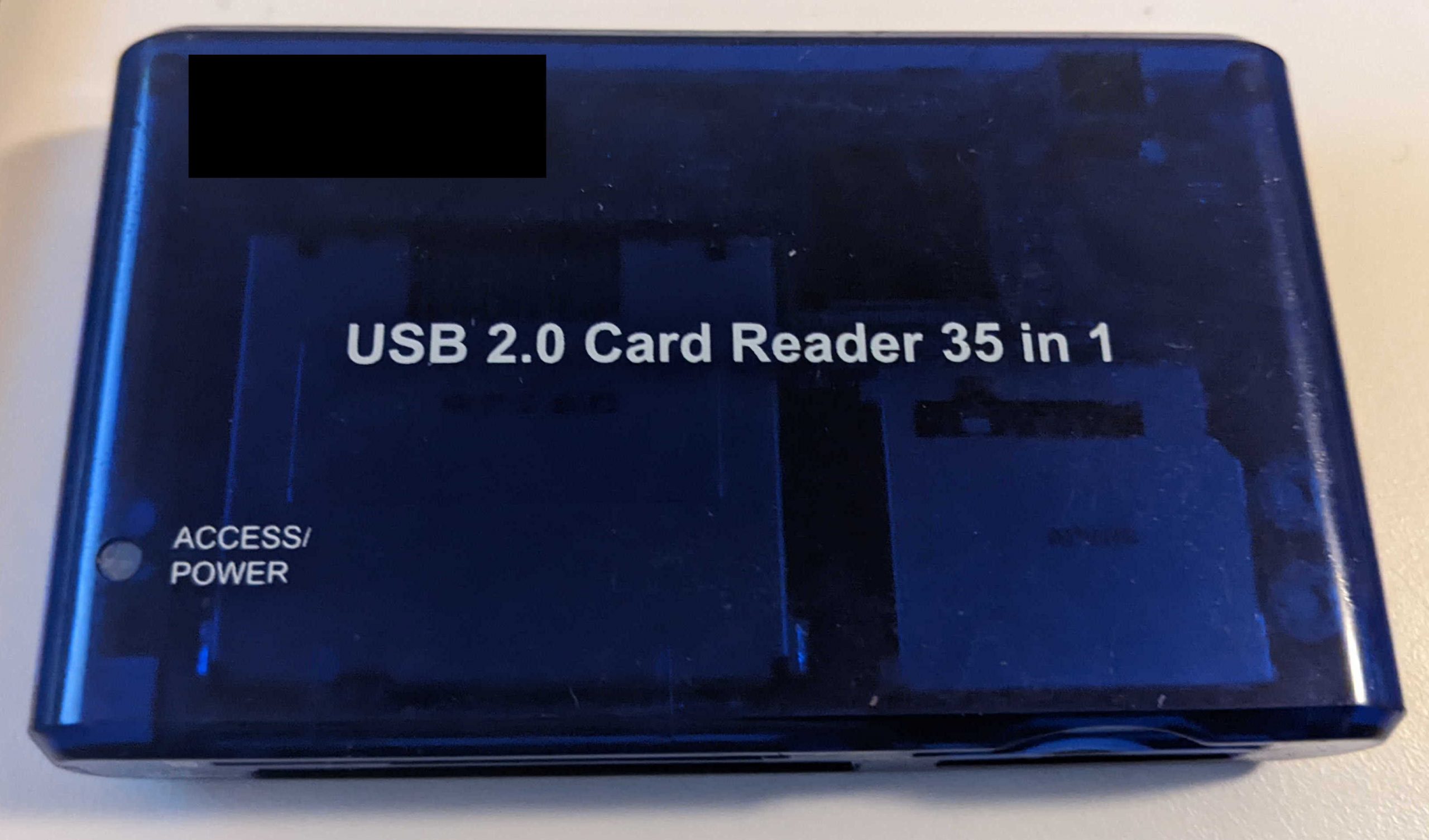
While I’m waiting for the delivery of some random hardware from China, I will start with a couple of useful tools and tricks applied to an old USB card reader. Here it is:
And this is how it looks without the external cover:
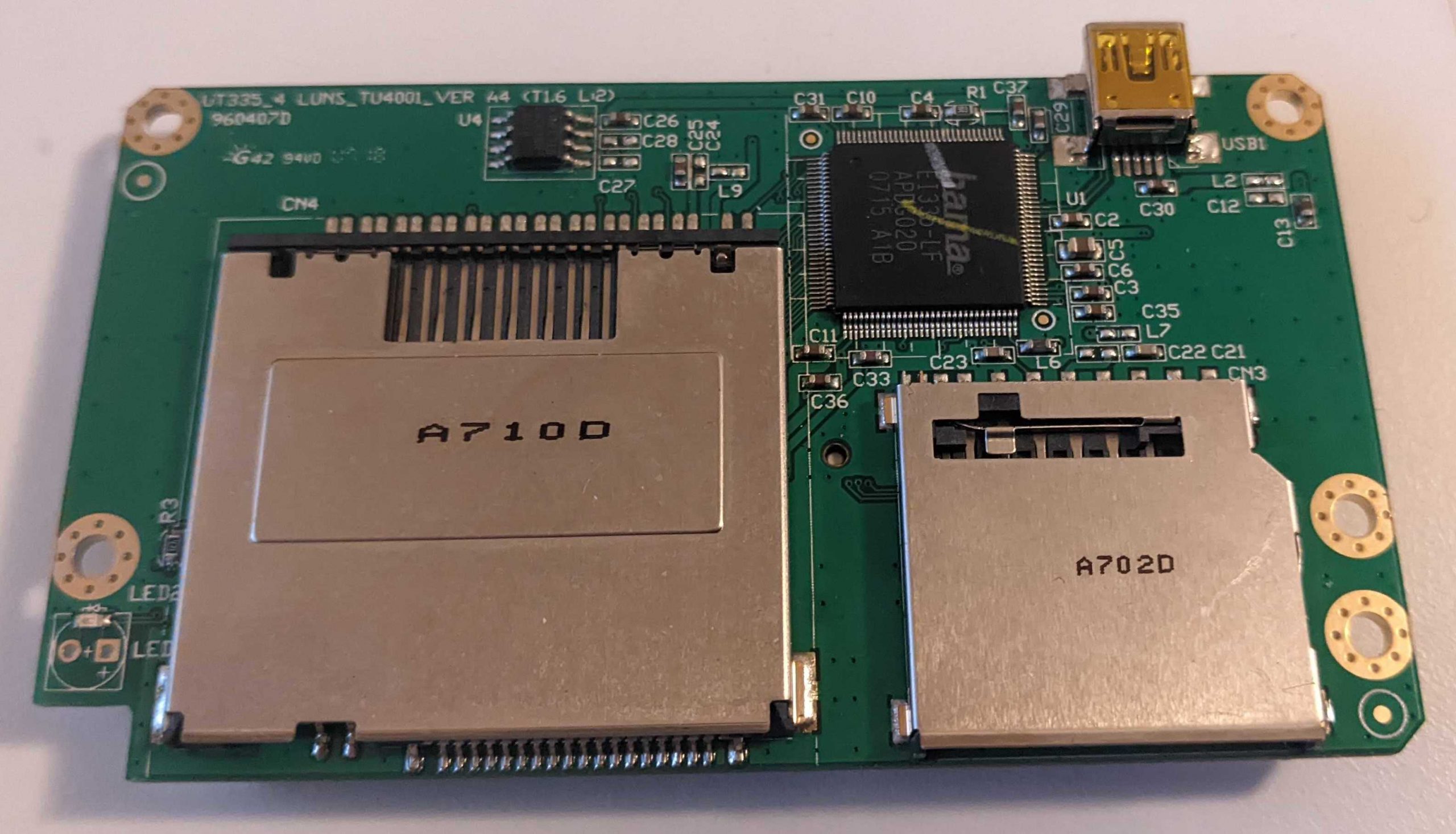
When we are facing an unknown platform like this one, the first step should always be to identify all chips and components on the board.
If we are lucky, our device has a wireless connection and it is sold in the United States, it should have an identifier named FCC ID printed somewhere on the product or on its box. With this ID we can download a lot of useful documentation that is publicly available, mandatory for the legal sale in the US, including manuals, photos, and technical details. We will maybe see some examples when we analyze a wireless device, but this is not the case.
Without technical documentation, we are on our own. Usually, most chips have an identifier printed on them, but this information is very hard to read. A useful tool is a digital microscope, that can be bought from a Chinese supplier for about 10-20 euros, and that can be connected to a laptop or a smartphone. With this device, we can easily take a picture of all the chips on the board and try to identify every component.
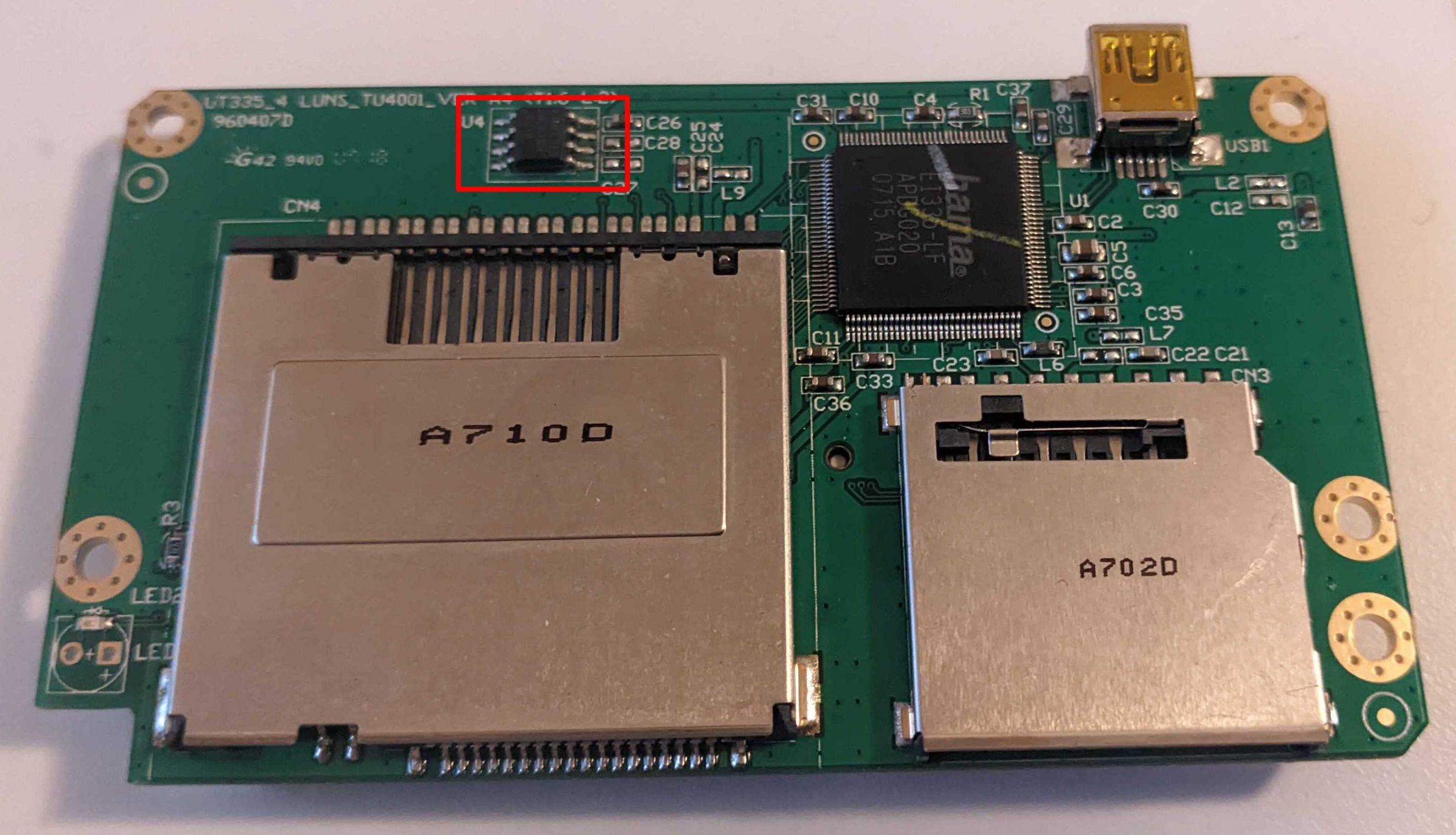
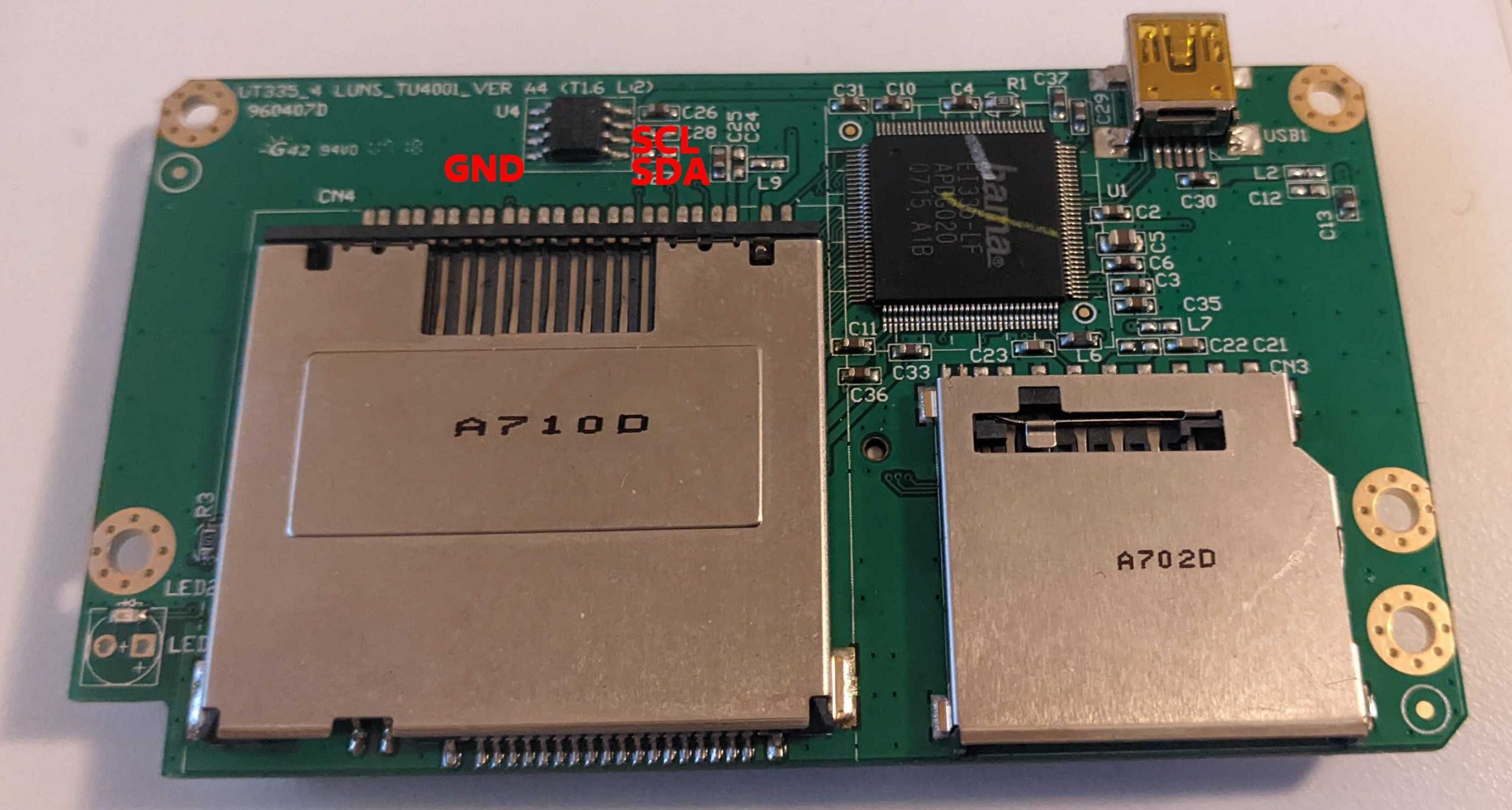
As an example, let’s have a closer look at the chip in the top-left side of the board:
With the digital microscope, we can read the identifier printed on the chip:
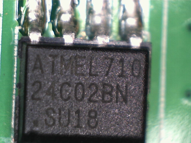
By searching the identifier with our favorite search engine, we can easily find its datasheet, that shows that it is a Serial EEPROM memory with 2K of storage that communicates using the I2C protocol (Two-wire). The same document gives us the details of the chip connection pins.

We found an EEPROM memory. We can try to read its content using the I2C protocol. I2C is a serial communication protocol that allows to connect on the same bus a large number of devices, each reachable from a specific address. It was invented in 1982 by Philips Semiconductors (now NXP). It requires only two PINs, one for data and one for the clock, necessary for synchronization.
Every chip usually has a mark near the first PIN, necessary to identify the side of the chip. If you look at the above picture, you can see this mark in the bottom-left side of the chip. Using this mark and the datasheet, we can easily identify all the PINs and we can confirm the correctness of our analysis with the help of a multimeter in continuity mode. To verify the position of the Ground PIN (GND) it is sufficient to connect one probe of the multimeter to one of the metal components (usually connected with GND) and the other first to the bottom-left PIN of the chip and then to the top-right (see the previous article linked at the beginning of this post for more details).
So, we now know the position of all the PINs we need to communicate with the EEPROM using the I2C protocol:
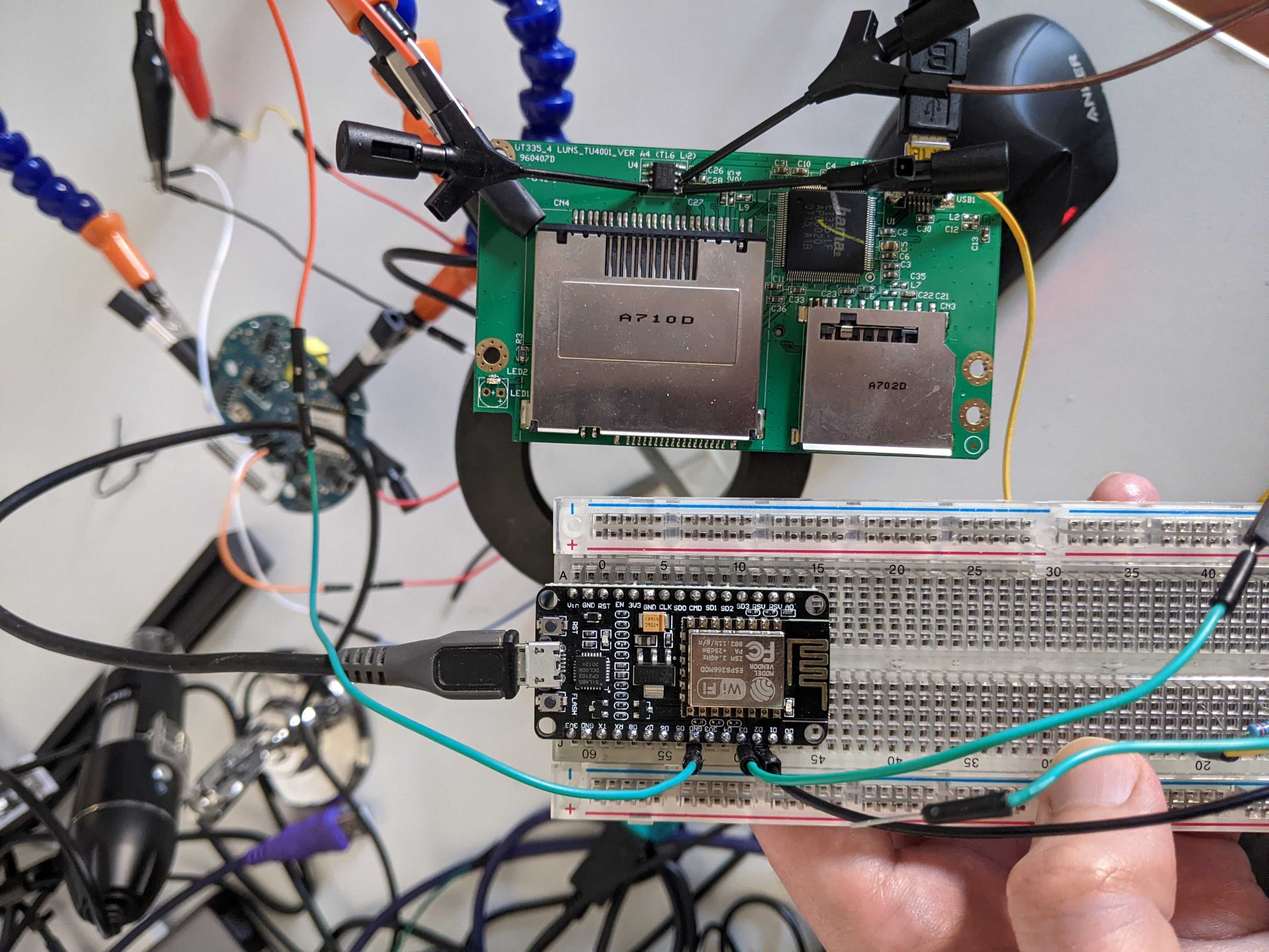
To read (and maybe write) the content of the EEPROM we can use many different tools. One of the most used is the old but trusted Bus Pirate.
But let’s pretend for a moment that we have no idea of the location of the I2C PINs. A few years ago, Silvio Cesare publicly released a great tool named BUSSide Badge (sources on GitHub). The badge is composed by a NodeMCU v2 module (a couple of euros from Chinese suppliers) and a printed PLC (hard to find but not necessary to use the tool). This ultra-cheap badge has many functionalities, including:
- Discover UART pinout
- Discover SPI pinout
- Discover I2C pinout
- Discover JTAG pinout
- UART passthrough
- SPI flash read/write
- I2C slave discovery
- I2C flash read/write
After having flashed the BUSSide firmware on the NodeMCU v2 (directly via USB following the instructions in the repository), first we have to connect the Ground (GND) of the target chip with the GND of the BUSSide, and then we can connect all unknown PINs of our EEPROM to arbitrary NodeMCU PINs from D1 to D8 (BUSSide refers to GPIO 1-9 that respectively are NodeMCU D0-D8, but it is better not to use D0 because many BUSSide features don’t work on that PIN). In this demo I connected only the two correct ones because I was at home with only a few connectors (and sorry for the hardware mess in the background; it is the subject of the next article 🙂 ):
Now, if we can connect the USB card reader and the BUSSide to two USB ports and run the BUSSide we have the following output:
$ sudo python2 Client/busside.py /dev/ttyUSB0
+++ Connecting to the BUSSIde
+++ Sending echo command
+++ OK
[...]
> i2c discover pinout
+++ Sending i2c discover pinout command
+++ Connecting to the BUSSIde
+++ FOUND 0 I2C interfaces
+++ SUCCESS
The BUSSide could not find any I2C interface, probably because in order to find the I2C interface the BUSSide needs I2C communications. The card reader reads from the EEPROM only when it boots. So, in order to detect the interface we can try to execute the discovery command right after the connection of the card reader to the USB port (it may take a few tries). When the operation succeeds, the output is the following:
$ python2 Client/busside.py /dev/ttyUSB0
+++ Connecting to the BUSSIde
+++ Sending echo command
+++ OK
[...]
> i2c discover pinout
+++ Sending i2c discover pinout command
+++ Connecting to the BUSSIde
+++ FOUND 1 I2C interfaces
+++ I2C interface FOUND
+++ I2C SDA at GPIO 4
+++ I2C SCL at GPIO 3
+++ SUCCESS
After having identified the port, it is necessary to find the slave address of our EEPROM (I2C allows to connect multiple devices on the same bus, each identified by a specific address) as follows:
> i2c discover slaves 4 3
+++ Sending i2c slave discovery command
+++ 1 I2C slave addresses
+++ I2C slave address FOUND at 80
+++ SUCCESS
And now, the BUSSide can be used to read the EEPROM and save the content in an output file, supplying the address of the slave just found and the size to read (256 bytes, according to the datasheet):
> i2c flash dump 4 3 80 1 256 /tmp/i2cDump.bin
+++ Dumping I2C
+++ SUCCESS

> quit
Bye!

$ hexdump -C /tmp/i2cDump.bin
00000000 43 52 31 ff 13 07 03 30 fa 07 01 50 00 00 89 08 |CR1....0...P....|
00000010 00 01 03 03 02 ff ff 01 00 02 02 04 03 00 ff ff |................|
00000020 00 01 02 03 04 05 06 07 40 0a 70 0b 0c 0d 0e 0f |........@.p.....|
00000030 00 00 00 00 00 00 00 00 00 00 00 00 00 00 00 9d |................|
00000040 55 53 42 20 43 46 20 52 65 61 64 65 72 00 00 00 |USB CF Reader...|
00000050 55 53 42 20 53 44 20 52 65 61 64 65 72 00 00 00 |USB SD Reader...|
00000060 55 53 42 20 4d 53 20 52 65 61 64 65 72 00 00 00 |USB MS Reader...|
00000070 55 53 42 20 53 4d 20 52 65 61 64 65 72 00 00 00 |USB SM Reader...|
00000080 00 00 00 00 00 00 00 00 00 00 00 00 00 00 00 00 |................|
00000090 4d 69 6e 69 20 53 44 20 52 65 61 64 65 72 00 00 |Mini SD Reader..|
000000a0 00 00 00 00 00 00 00 00 00 00 00 00 00 00 00 00 |................|
000000b0 30 30 30 30 30 30 30 30 30 30 30 30 31 30 30 00 |000000000000100.|
000000c0 00 00 00 00 00 00 00 00 47 65 6e 65 72 69 63 00 |........Generic.|
000000d0 00 00 00 00 00 00 00 00 00 00 00 00 00 00 00 00 |................|
000000e0 4d 61 73 73 20 53 74 6f 72 61 67 65 20 44 65 76 |Mass Storage Dev|
000000f0 69 63 65 00 00 00 00 00 ff ff ff ff ff ff 63 ff |ice...........c.|
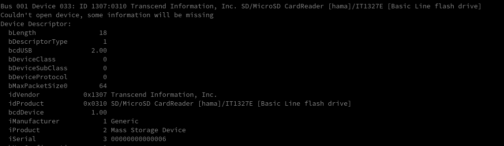
We can see how the data contained in the EEPROM is used with the “lsusb -v” command, as follows:
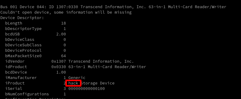
We can also try to change the data stored on the EEPROM. First, let’s edit our dump, changing the string “Mass Storage Device” in “hack Storage Device” with our favorite hex editor. Our modified dump is the following:
$ hexdump -C i2cDumpEdited.bin
00000000  43 52 31 ff 13 07 03 30  fa 07 01 50 00 00 89 08  |CR1....0...P....|
00000010  00 01 03 03 02 ff ff 01  00 02 02 04 03 00 ff ff  |................|
00000020  00 01 02 03 04 05 06 07  40 0a 70 0b 0c 0d 0e 0f  |........@.p.....|
00000030  00 00 00 00 00 00 00 00  00 00 00 00 00 00 00 9d  |................|
00000040  55 53 42 20 43 46 20 52  65 61 64 65 72 00 00 00  |USB CF Reader...|
00000050  55 53 42 20 53 44 20 52  65 61 64 65 72 00 00 00  |USB SD Reader...|
00000060  55 53 42 20 4d 53 20 52  65 61 64 65 72 00 00 00  |USB MS Reader...|
00000070  55 53 42 20 53 4d 20 52  65 61 64 65 72 00 00 00  |USB SM Reader...|
00000080  00 00 00 00 00 00 00 00  00 00 00 00 00 00 00 00  |................|
00000090  4d 69 6e 69 20 53 44 20  52 65 61 64 65 72 00 00  |Mini SD Reader..|
000000a0  00 00 00 00 00 00 00 00  00 00 00 00 00 00 00 00  |................|
000000b0  30 30 30 30 30 30 30 30  30 30 30 30 31 30 30 00  |000000000000100.|
000000c0  00 00 00 00 00 00 00 00  47 65 6e 65 72 69 63 00  |........Generic.|
000000d0  00 00 00 00 00 00 00 00  00 00 00 00 00 00 00 00  |................|
000000e0  68 61 63 6b 20 53 74 6f  72 61 67 65 20 44 65 76  |hack Storage Dev|
000000f0  69 63 65 00 00 00 00 00  ff ff ff ff ff ff 63 ff  |ice...........c.|
Now we can write our edited dump using BUSSide i2c write command, similar to the one used to dump the EEPROM content (“i2c flash write 4 3 80 1 256 /tmp/i2cDumpEdited.bin“). After unplugging/plugging again the card reader, we can see the result of our modifications using the “lsusb -v” command again:
The same dump operation can be executed also with tools like Bus Pirate. After connecting GND, SDA, and SCL PINs (like before) and plugging Bus Pirate to the USB port, we can connect to it using any serial terminal client (e.g., moserial, screen, etc.):
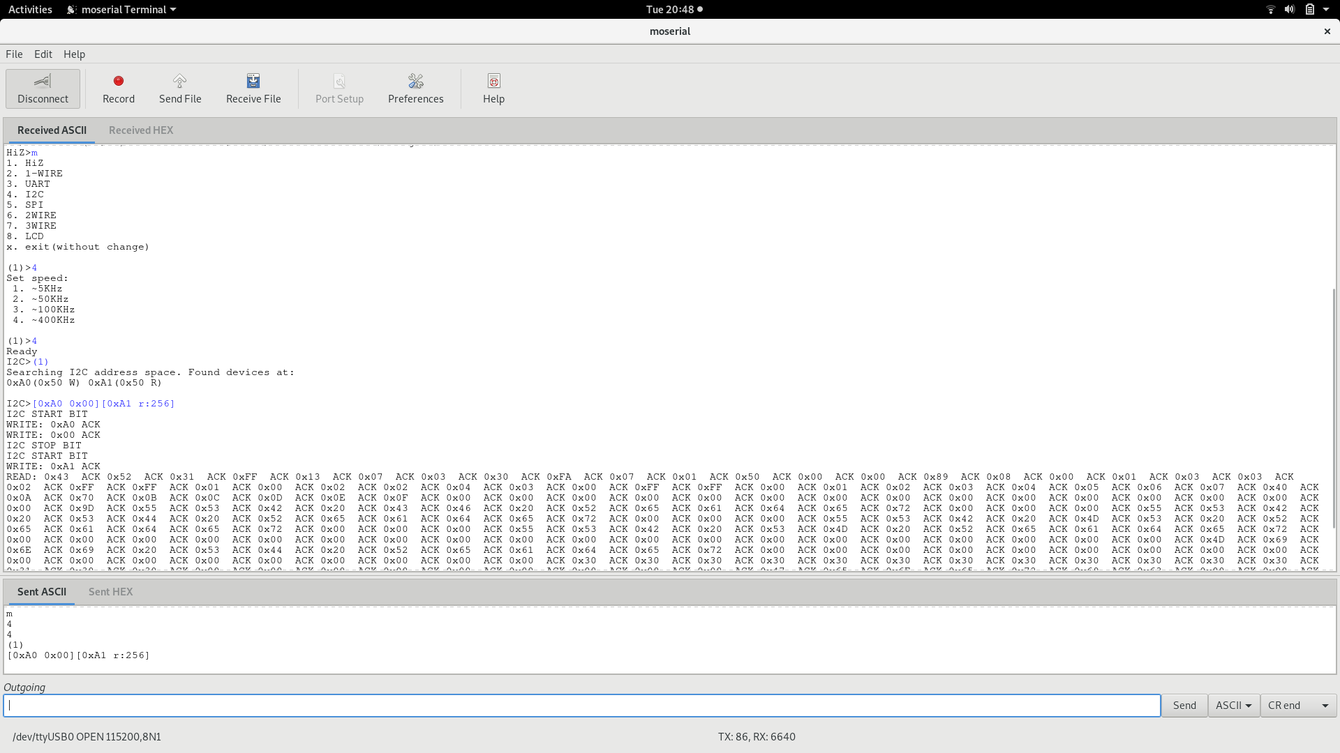
The commands executed in the previous picture in order to dump the EEPROM memory are the following (refer to Bus Pirate documentation for further details):
- m -> Set mode
- 4 -> Select I2C
- 4 -> Select 400Khz of speed
- (1) -> Scan I2C address space, found 0xA0 (write) and 0xA1 (read)
- [0xA0 0x00][0xA1 r:256] -> Go to the first byte (“[0xA0 0x00]”) and read 256 bytes (“[0xA1 r:256]”); 2048 bit is the size of the EEPROM according to the datasheet
If we want, we can also modify this EEPROM memory as we did with the BUSSide, as follows:
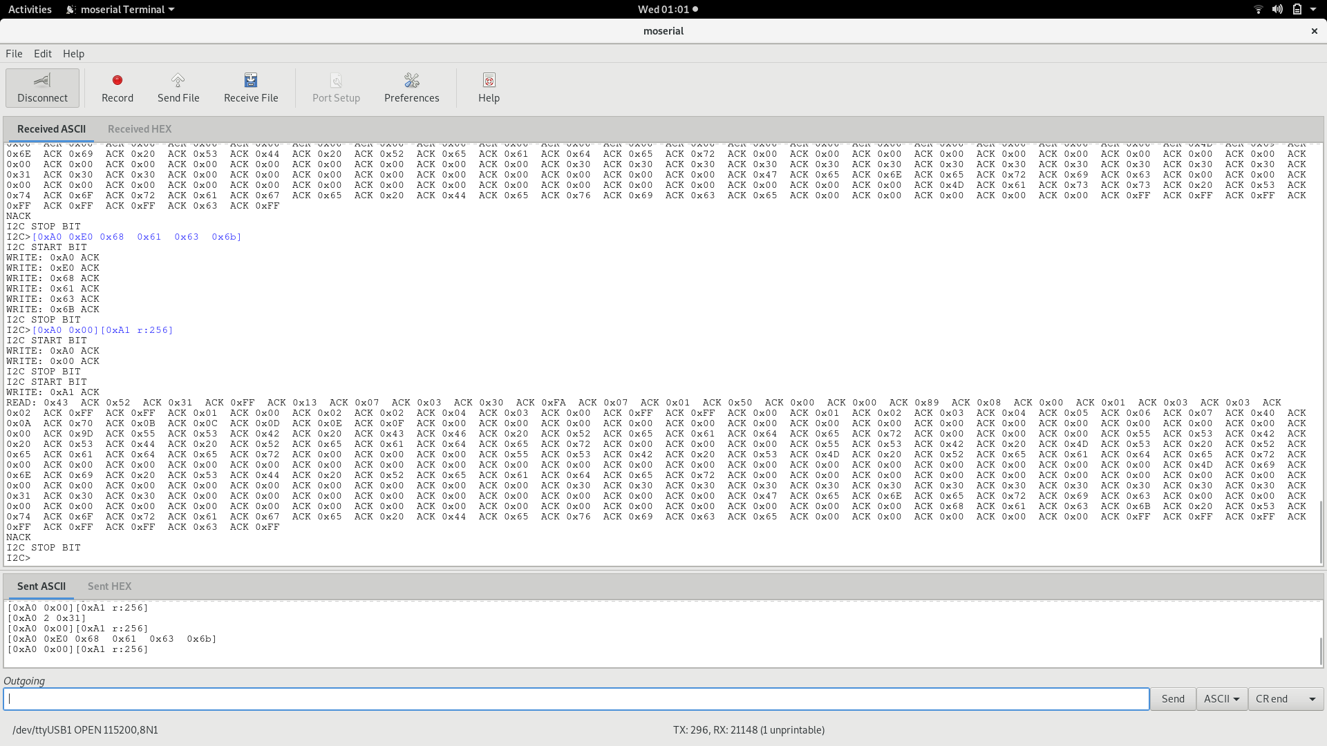
The commands executed are:
- [0xA0 0xE0 0x68 0x61 0x63 0x6b] -> Write in address 0xE0 (224° byte) the bytes 0x68 0x61 0x63 0x6b (“hack” in ASCII); previous content was “Mass”
- [0xA0 0x00][0xA1 r:256] -> Read again the EEPROM value (to check the output of the previous command)
And for this post that’s all. I will try to publish the next one on this topic before the next two years! 🙂
Cheers!