Disclaimer: as many other security researchers approaching IoT, I have a background in computer science and I started to work on these subjects with little knowledge about electronics and often with a “YOLO” approach (blame it on an old colleague of mine 🙂 ). So, it is definitely possible that many of the things you will read here can be inaccurate or can be done in a much better way, especially with more knowledge in the field. Sorry about that. I take advantage of this disclaimer to add a thing: pay particular attention when you put your hands on electronics, especially when you deal with cheap Chinese devices powered by 220V! Some capacitors can cause serious damages even if the device is not plugged into the electric socket!
So, after a couple of introductory articles, let’s start with a series of articles on an analysis executed on an unknown device. I received a Chinese smart alarm, clone of the Xiaomi Smart Home system, and it seemed perfect for the purpose. This is my target:
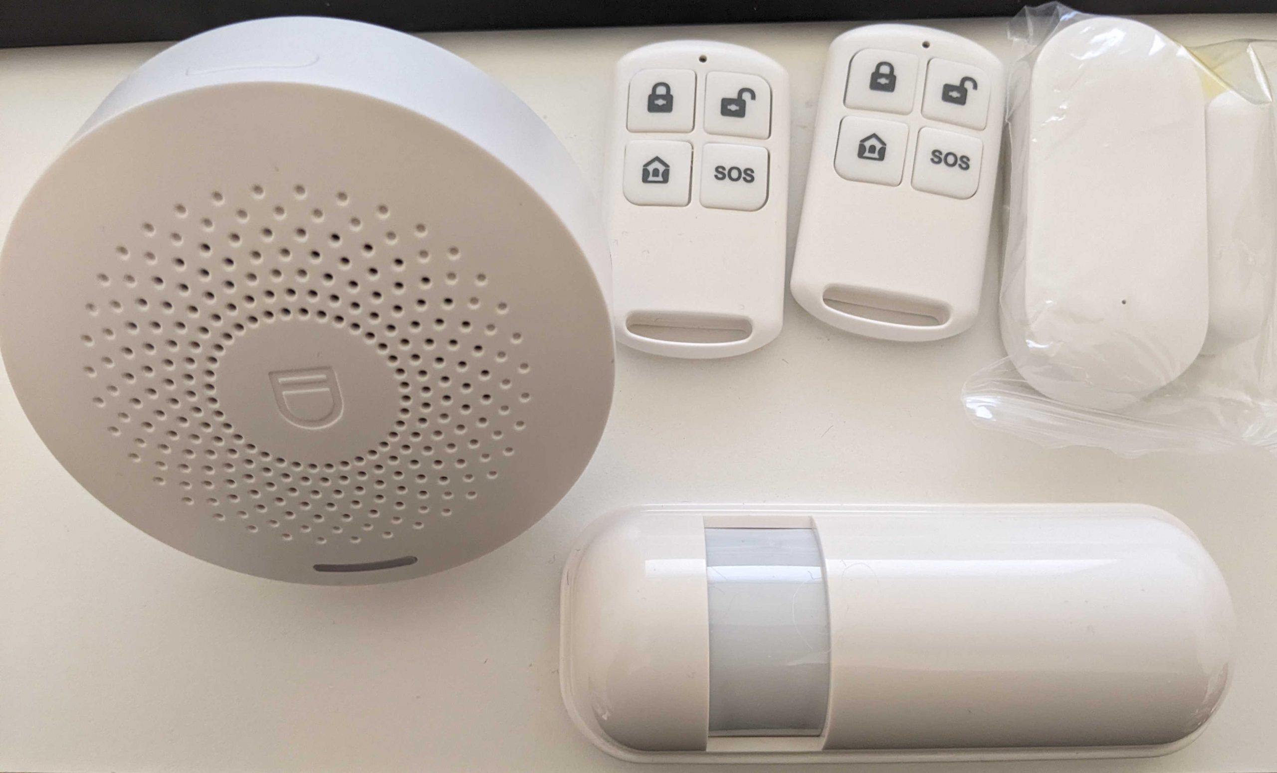
It includes the following components:
- A smart hub, which is the main device. It handles the alarm system, receiving the input from wireless sensors and remote controls. It has an on-board speaker for the siren. It is connected to the home WiFi network and it communicates with Cloud services. It can be configured using a specific Android application available on the Google Play Store.
- A door sensor, which sends an alarm when the door is opened (battery powered).
- A motion sensor, which sends an alarm when something moves in front of the sensor (battery powered).
- Two remote controls, to enable/disable the alarm (battery powered).
With such a device, there are a lot of things that we can analyze to understand how they work and to find any security issues, like:
- Communications between the sensors and the hub.
- Communications between the remote controls and the hub.
- Communications between the hub and Cloud services.
- Communication ports and protocols used by all hardware components.
- Debugging ports (if any) present on hardware.
- The firmware of the main chip (or chips).
- The code of the mobile application.
- Communications between the mobile application and the Cloud provider.
- And so on…
First step: setup our testing environment and test the device. So, I downloaded the mobile application on a test Android device and I paired it with the smart alarm. The two sensors (door sensor and motion sensor) were already configured, as were the two remote controls. Only the motion sensor and one of the remote controls worked correctly but it’s a 30$ alarm system, I would say that I can be satisfied. 🙂
The paring procedure between the hub and the Cloud can be also interesting to analyze, but I can reset the device and repeat the procedure at another time. It is better to be sure that all is working correctly before starting the analysis.
Component enumeration
Let’s dig more in depth on our device. First, our device has a wireless connection. If we are lucky, it may have an identifier named FCC ID printed somewhere on the product or on its box. With this ID we can download a lot of useful documentation that is publicly available, mandatory for the legal sale in the US, including manuals, photos, and technical details. But unfortunately this is not the case. Our device does not have an FCC ID (nor a brand name or anything else 🙂 ).
Plan B: open the device.
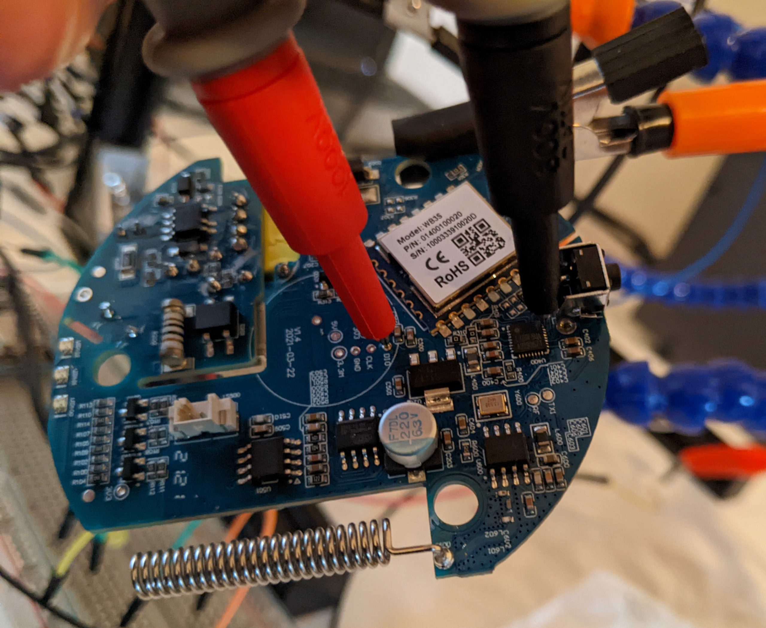
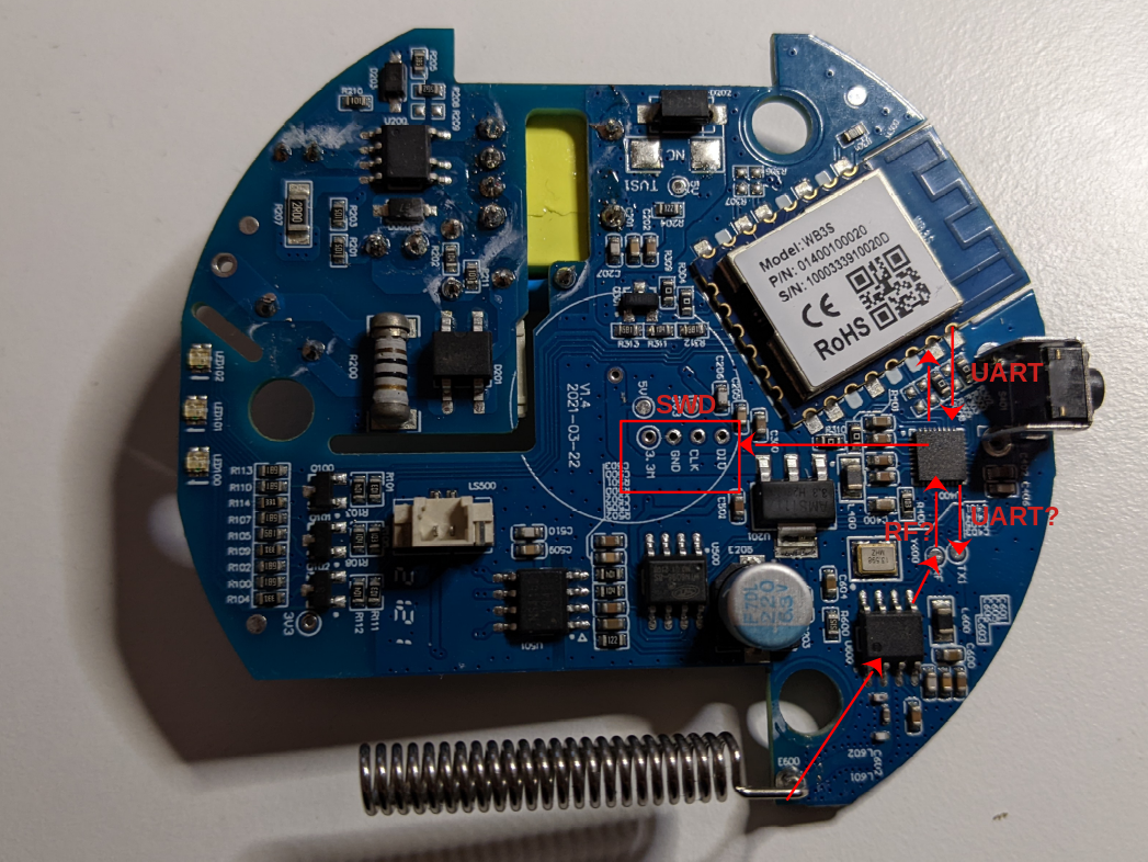
After unplugging the device from the electric socket and opening the plastic we can reach the main board, that is connected on one side with the electric plug and on the other to the speaker:
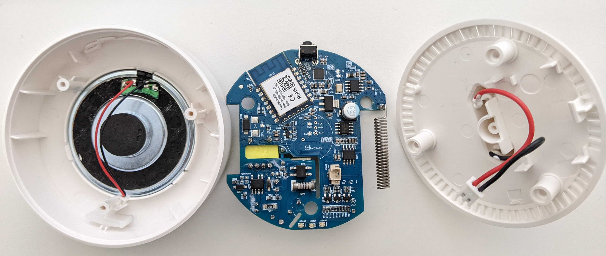
Safety tip: this kind of electronic devices usually work at 3.3V or 5V (maybe some components at something more). So the 220V alternate current usually is transformed to a 5V or similar direct current. If our device uses an external power adapter, usually only a few Volts reach the electronic device (you should be able to read the exact amount on the power adapter). In this example, we have the device directly plugged in the electric plug and the voltage is reduced directly on the board by specific electric components. Well, I think that it is better to avoid putting the hand on a 30$ Chinese device plugged on 220V. 🙂 After component enumeration (that is executed with the device unplugged) we will try to find a better way to power-up the device without the risks of the 220V. One more thing: pay attention to the capacitors. Big capacitors can hold high voltage for many hours after they are unplugged from the electric plug and can be dangerous. It is rare to find such capacitors in small electronics, but in case of doubt a good way to safely discharge a capacitor is to hold a resistor with a pair of pliers (maybe a high-wattage resistor at 100 Ohm or similar) and keep the legs of the resistor to the capacitor contacts for a few seconds. 😉
The board presents many different chips. To understand their purpose we can search for their datasheet online. Usually they have an identifier written on them, but it can be hard to see to the naked eye. With the help of a digital microscope, which can be bought from a Chinese supplier for about 10-20 euros, we can easily take a picture of all the chips on the board.
Then we can try to identify every component by searching for information and for their datasheet with our favorite search engine (sometimes it is simple, sometimes it is harder; keep in mind that the model name could be only a portion of the string printed on the chip).
Most chips present on the board are not very interesting from a security point of view (regulators, transformers, …) while other can be juicy (microcontroller, memories, …). As an example, in our board we found the following components related to power supply, current and audio, that we will probably skip:
- MB6S: bridge rectifier, converts AC current into DC currents.
- FSD3783A: power supply IC.
- NS4150: audio amplifier.
- WTN6096-8S: voice chip.
- SS24: diode.
- AMS1117: voltage regulator.
- JZPR30: datasheet not found, but likely used to communicate with alarm sensors (see later).
The following two components, on the contrary, look very promising:
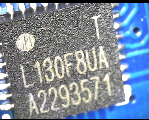
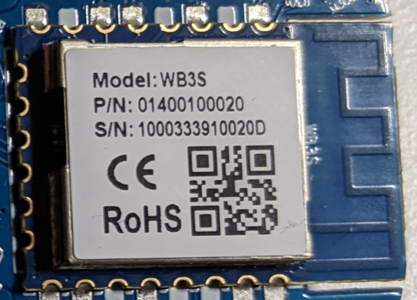
After searching these models online we found the chip information and their datasheets:
- HDSC HC32L130F8UA (datasheet in Chinese here, thank you Google translate!), 32-bit ARM Cortex M0+ microcontroller.
- tuya WB3S (datasheet here), low-power embedded WiFi and Bluetooth LE Dual protocol module. The reported datasheet is of a tuya module. Under the metal enclosure there is the microcontroller used by tuya for their module. Connecting directly to it could be better for some analysis, because only a subset of its PINs are reachable from the tuya module, but for the moment it is not necessary because we are interested only in its interfaces offered to other components of the board.
Beside the chips, there are some interesting set of pins (ports), that probably have been moved on the board for debugging purposes:
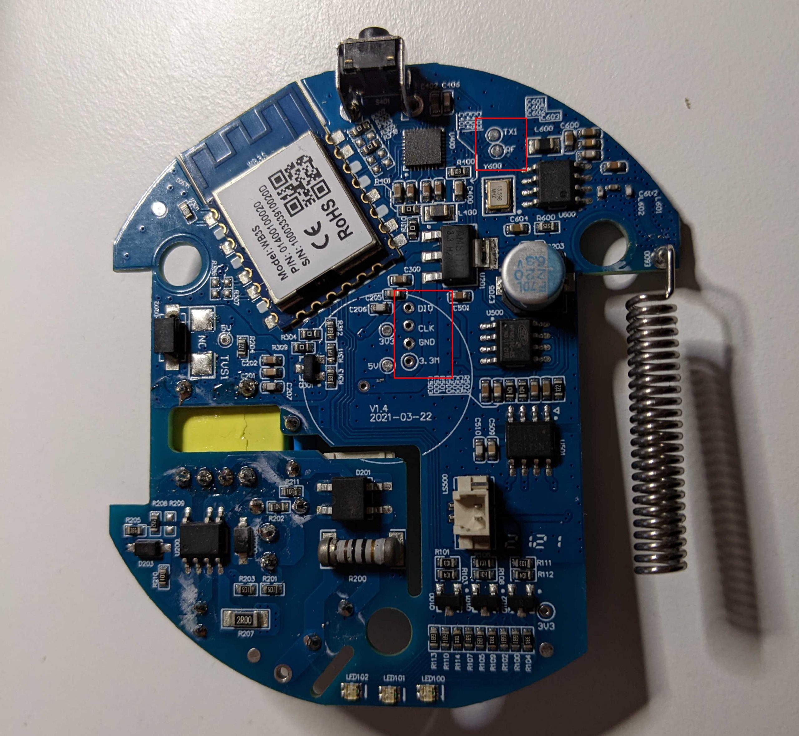
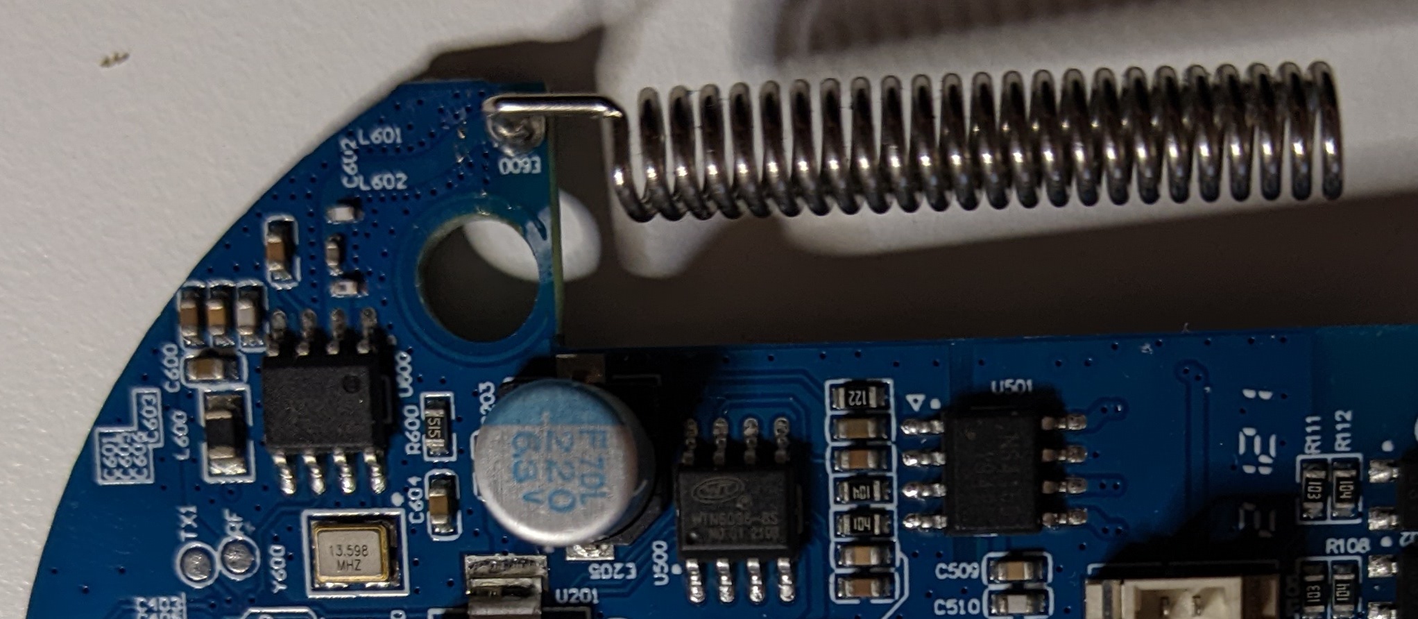
Finally we have an external antenna, probably used to communicate with the sensors and the remote controls:
Preliminary analysis with the device powered off
Before powering the device on, we can try to better understand how the most interesting chips we found are connected between them and with the ports, using the datasheets and a multimeter in continuity mode.
One approach can be to follow the tracks (the “lines” on the two sides of the PCB that connect all the PINs and components) but there are types of PCB (named multi-layer PCB) that have tracks that are not visible from the two sides of the board (and anyhow it requires good eyes and tons of patience…). A faster and more focused approach is to touch two points with a multimeter in continuity mode. If it beeps, they should be directly connected.
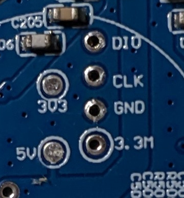
Let’s start with the port in the center of the board. Beside GND and voltage PINs (3.3 and 5), it has two PINs named CLK and DIO.
If we look at the datasheet of the HC32L130F8UA microcontroller, we can see two PINs with similar names:
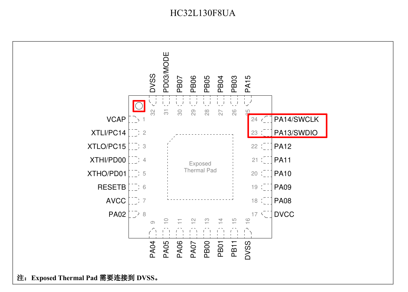
So, we ca try to use our multimeter to check if CLK PIN on the PCB is connected to PA14/SWCLK and if DIO PIN is connected to PA13/SWDIO, which confirms our assumption (the highlighted point in the top-left corner of the datasheet is present also in the chip: its purpose is to understand the chip orientation):
Thanks to the datasheet, we know that these PINs are a SWD port (Serial Wire Debug). The SWD port is an ARM debugging port that uses the same protocol of the JTAG debugging interface with only two PINs. A debugging port (if enabled or if we can enable it, because it can be disabled) is very valuable because, among other great benefits of being able to debug the code, it can be used to dump the content of the flash memory. We will definitely try this operation later, when we will power on the device.
Secondly, let’s check if we can find a connection between the WiFi module and the ARM microcontroller. From the WiFi module datasheet we can see that the module has two UART ports, the second one according to the documentation is unavailable to customers:
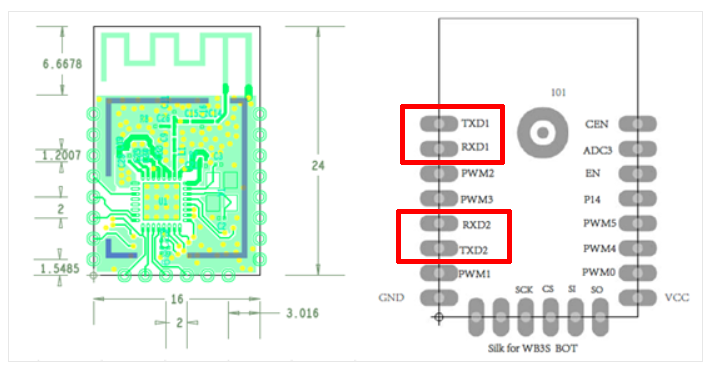
Using the multimeter we can confirm that the two PINs of the first UART are connected to PA09 and PA10 PINs of the ARM microcontroller (from the documentation these PINs can use the UART protocol). The two PINs of the second UART port of the WiFi module do not seem to be connected to any PIN of the ARM microcontroller (confirming what is stated in the WiFi module datasheet about the second UART port).
Now, let’s switch to the second port on the PCB. The second port contains a PIN named TX1 (potentially a UART PIN) and a PIN named RF (unknown for now, maybe Radio Frequency?).
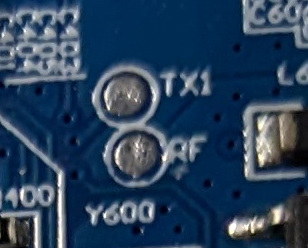
Thanks to the multimeter, we can verify that the TX1 PIN on the PCB is connected to the PA04 PIN on the ARM microcontroller (from the documentation this PIN can be a UART TX PIN) and the PCB RF PIN is connected to the PA02 port.
Finally, let’s have a look at the antenna:
Near the antenna (bottom-left) we can see the following chip:
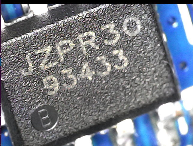
I did not find the datasheet of this chip but:
- One of its PINs is connected to the antenna, as verified with the multimeter.
- One of its PINs is connected to the “RF” PIN on the PCB we just saw (that is also connected to a PIN of the ARM microcontroller), also verified with the multimeter.
- The second line of the model is 93433. Maybe the antenna can be a 433Mhz antenna? A very common radio frequency for remote controllers and similar device.
So, the output of this initial analysis is the following (we will verify its correctness later):
Giving power to the device
The next step is to try to find a way to give power to the device, without using the electric socket. For this task will use an Adjustable DC power supply (an AC-DC converter in which it is possible to set an output Voltage), but first we will need to determine how many Volts it needs and where we can connect the power supply. So, let’s try to understand how the device is powered from the electric socket.
Following the tracks with the help of our multimeter in continuity mode, we find that the connector of the plug reaches the following chip (after passing a capacitor and a resistor):
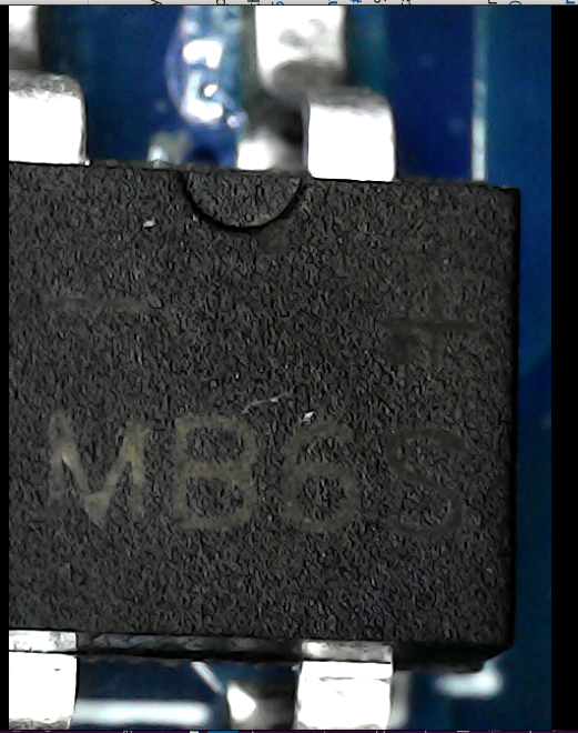
From its datasheet (MB6S) we discover that it is a rectifier, that rectifies the AC current in DC current. Current that exits from this chip is direct but still at high voltage.
The MB6S chip is then connected to the following transformer:
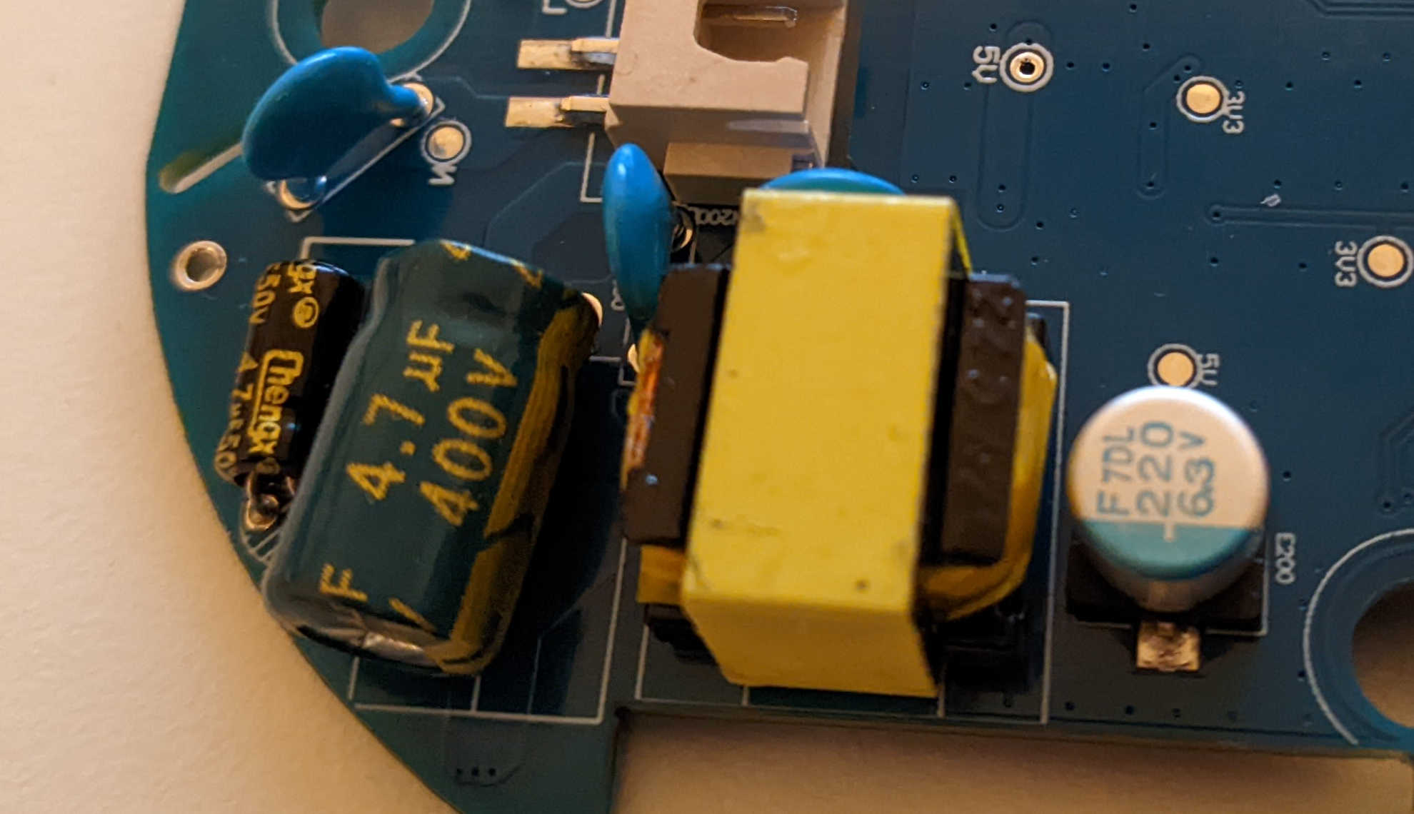
The output voltage of the transformer is probably the value that we need to give the correct power to the device without using the electric socket. Maybe there is a way to understand the output value from the capacitors near the transformer, but honestly I don’t know. So I connected the device to the electric socket and with caution I measured the voltage in output to the transformer using the multimeter in voltage mode (the ground can be connected to any metal component or GND pin of the board). The value detected was 5 Volt.
The output PIN of the transformer is directly connected to the following chip:
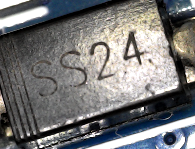
Its datasheet says that it should be a diode, a component that allows the current to flow only in one direction. This kind of components are often use to protect electronic components, preventing current to flow in the wrong direction. It could be a good point where put the VCC of our power supply. After unplugging the device from the electric socket, we can use the multimeter in the diode mode to check if the current flows only one-way. Unfortunately the current seems to flow in both ways (one less than the other), probably due to other tracks of the circuit (I don’t know).
Well, even if the diode does not fully protect the circuit, it is still a Chinese cheap device and I think I can take a little risk and connect the VCC of the power supply after the diode. 🙂
So, the VCC of the power supply has been connected after the diode and the GND of the power supply to one of the GND of the PLC (I used the GND of the SWD port in which I put a jumper), with the power supply set to 5V:
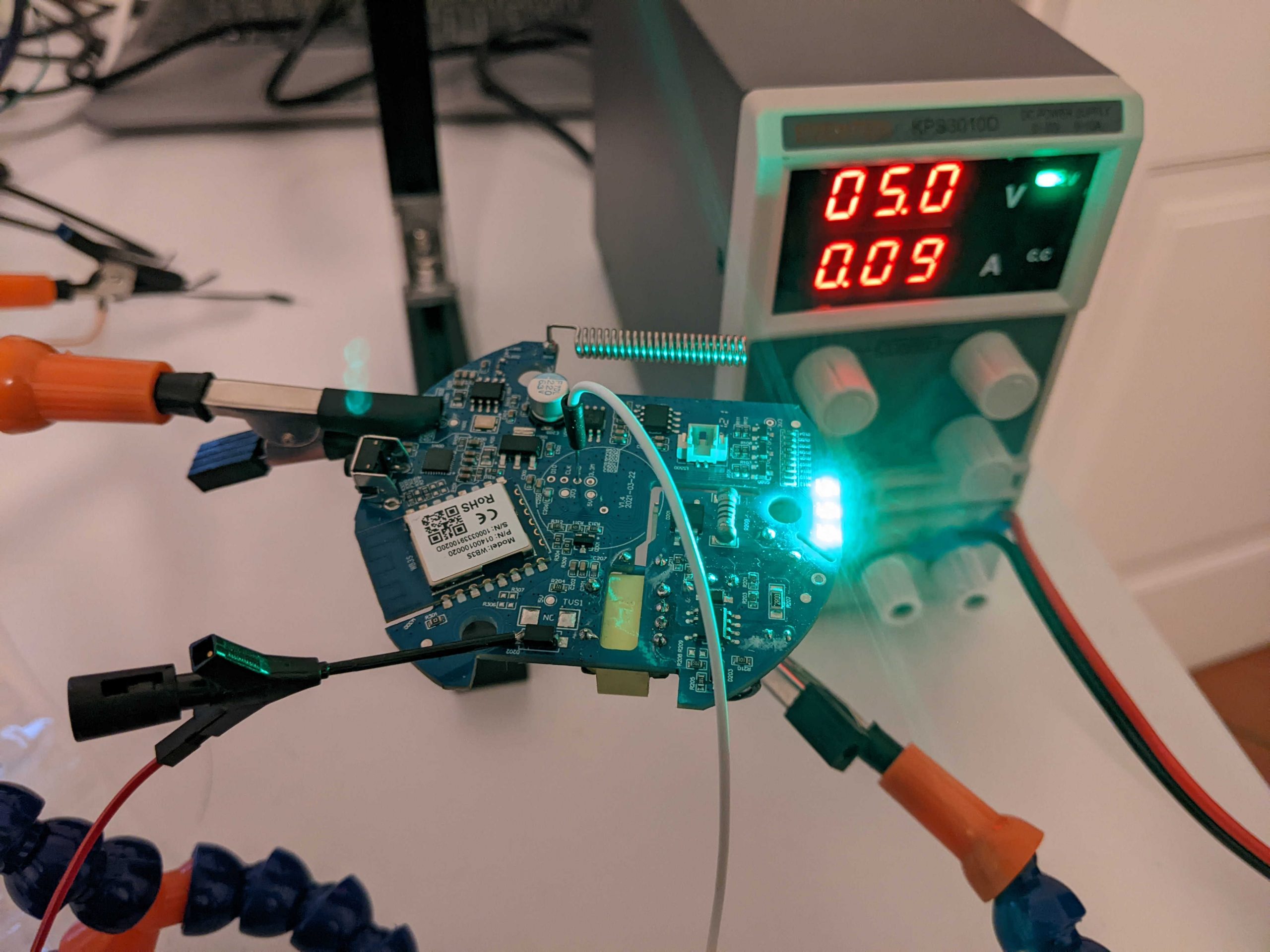
I tried the alarm device and it worked correctly. To be honest, when the device is turned on/off it sends alarms to the mobile application related to anomalies in the power supply, but if it continues to work correctly for me it is not a problem! 😀
Well, now we can start analyzing the running device, but for this article this is all. We will continue our analysis in the next one!
Cheers!