Disclaimer: as many other security researchers approaching IoT, I have a background in computer science and I started to work on these subjects with little knowledge about electronics and often with a “YOLO” approach (blame it on an old colleague of mine 🙂 ). So, it is definitely possible that many of the things you will read here can be inaccurate or can be done in a much better way, especially with more knowledge in the field. Sorry about that. I take advantage of this disclaimer to add a thing: pay particular attention when you put your hands on electronics, especially when you deal with cheap Chinese devices powered by 220V! Some capacitors can cause serious damages even if the device is not plugged into the electric socket!
In the first part of this analysis we identified some interesting things, among which the SWD port (Serial Wire Debug) of an ARM microcontroller. The SWD port is an ARM debugging port that implements the same protocol of the JTAG debugging interface using only two PINs.
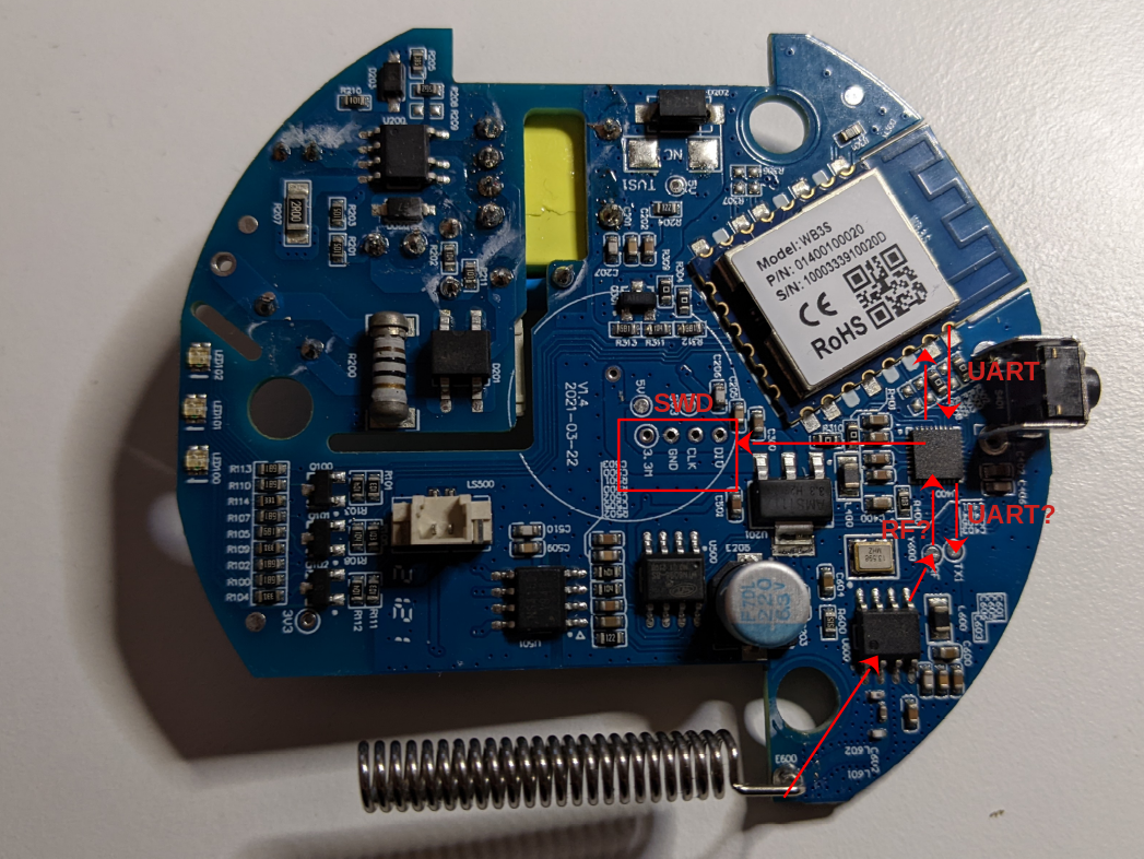
This debugging port (if enabled or if we can enable it, because it can be disabled) can be very valuable because, among other great benefits of being able to debug the code, usually it can be used to dump the content of the flash memory. That port belongs to an ARM microcontroller that probably handles the entire device. Consequently, being able to inspect its firmware can helps us enormously during our analysis.
The main issue now is: how can we obtain a debugging interface using the SWD port?
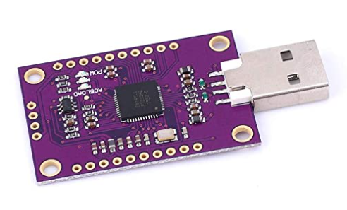
My first try was the OpenOCD (Open On-Chip Debugger) tool. OpenOCD is an open source project that provides on-chip programming and debugging support using a debug adapter. Various adapters can be used, including modules based on the FT232H chip (datasheet here). These modules are cheap (about 10€ from Chinese stores) and offer many different connections directly from the USB, among which UART, I2C, SPI, JTAG, and SWD.
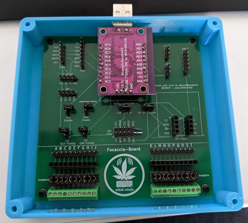
Luca Bongiorni (an Italian security researcher) created a board named Focaccia-Board with the purpose of providing a more comfortable environment when working with this module. This board has separate PINs for each connection, supports sockets and clips and has some sets of multipurpose PINs that can help keep order between cables and connections. He released all the stuff necessary to build a Focaccia-Board and it also possible to buy one from a Chinese seller on AliExpress (link on his GitHub repository). This is my board (the case is 3D printed, the STL file is in the Focaccia-Board GitHub repository):
OpenOCD complies with the remote gdbserver protocol and using GDB we can easily dump the content of the flash memory.
To use OpenOCD on a target it is necessary to have two configuration files: one for the adapter that we will use and one for the target chip. The configuration file to use the FT232H module with the SWD protocol is supplied with OpenOCD, but unfortunately I could not find the configuration file for the HC32L130F8UA 32-bit ARM Cortex M0+ microcontroller.
After some searching, I found out that my chip was supported by Keil MDK. Keil MDK is a software development environment for ARM Cortex-M based microcontroller devices, that offers many different tools including a debugger. HDSC, the vendor of the target ARM M0+ microcontroller, released the MDK Device Family Pack files (extension .pack) that allow to use the Keil MDK environment on its products.
In order to connect our target microcontroller to Keil MDK, it is necessary to have a debug adapter supported by it. Keil MDK supports many different debug adapters, including ULINK (device produced by Keil company), Segger J-Link, ST-Link, and many others. Some of these adapters are more expensive, other less (and many of them have Chinese clones). For our purposes a cheap device is more than enough (an ST-Link v2 original device costs around 25$). I will use a Segger J-Link, but the procedure is the same for most adapters.
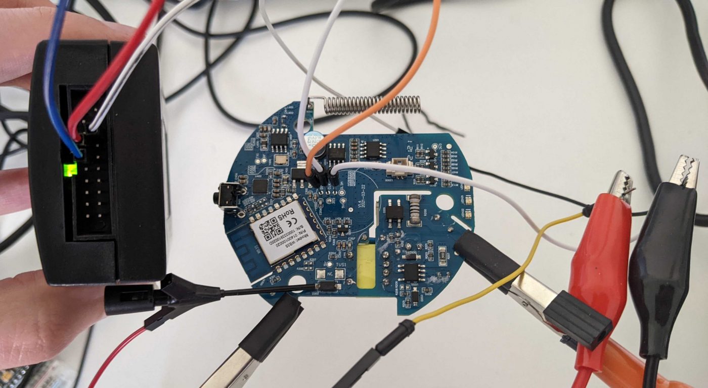
First, let’s have a look at the hardware connection. We have to connect the GND of our debug adapter to the GND of the target device and then the two PINs of the SWD port on the board, named DIO and CLK, respectively to the SWDIO and SWCLK ports of the debug adapter. With the Segger J-Link we have the following connections (forgive me for the jumpers directly put in the SWD port, but I’m at home and I don’t have headers of the right size to solder):
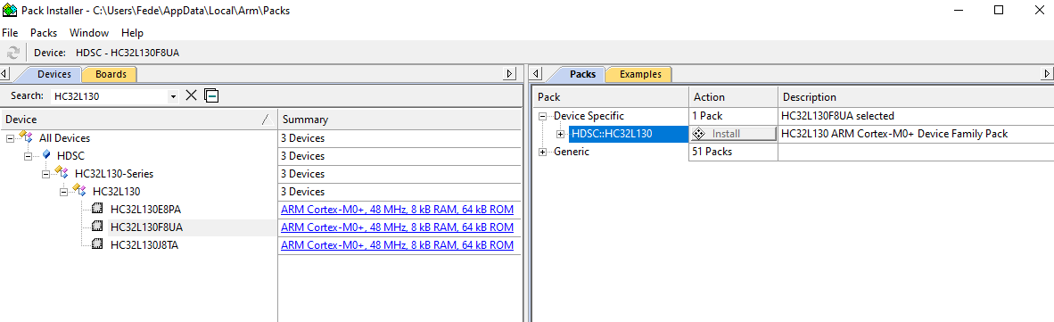
After installing the Keil MDK_ARM software, Keil opens the “Pack installer” tool (that later can be opened from Keil uVision, menu “Project” -> “Manage” -> “Pack Installer”). Here we can install the pack files that will allow Keil to properly communicate with our target modules, including the one for the target HDSC HC32L130F8UA microcontroller:
Before running the Keil tool we have to install the drivers of our debug adapter. The default location of the drivers is “C:\Keil_v5\ARM” (as an example, the driver for the Segger J-Link on a 64bit Windows OS is at “C:\Keil_v5\ARM\Segger\USBDriver\x64\”). Then we can run the Keil uVision 5 application.
First we have to create a new Project (menu “Project” -> “New uVision Project”), choose a name, and then select our target:

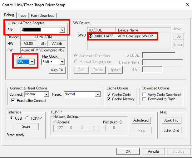
Then, we have to configure our debug adapter from the menu “Project” -> “Option for Target ‘Target 1′”. A popup appears with many configurations. This step should be executed with the debug adapter and the target device both powered up. In the “Debug” pane we can select if we want to use a simulator (on the left) or a physical adapter (on the right). We want to use a physical adapter, so we choose the right radio button and from the drop-down menu we select the J-LINK entry. We have to uncheck the below option “Load Application at Startup”, because we don’t want to run any application, but only execute the debugger to dump the microcontroller’s flash memory.

Before closing the configuration pane, it is necessary to configure the debug adapter by clicking on the “Settings” button near the drop-down menu we just configured. If the device is correctly detected by Keil, we should have an entry in the “SN” drop-down menu on the left with the serial number of our debug adapter. With the Segger J-Link we have to choose “SW” under “Port” and if all worked properly we should see an entry in the “SW Device” table (adapter configurations may be different if another debug adapter is used).
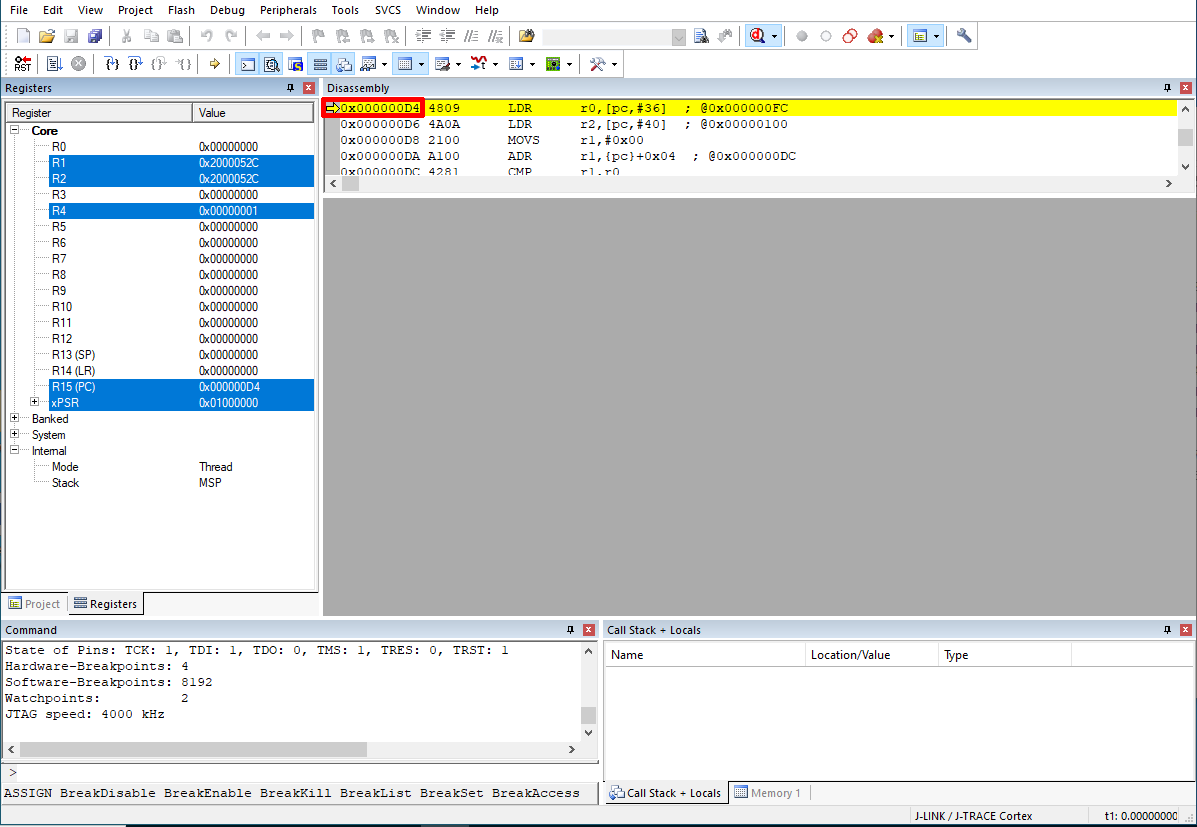
After confirming all configurations, we are ready to start the debugging phase by clicking on the the “Debug” -> “Start/Stop Debug Session” menu. When we select this option the microcontroller is reset and paused at the first instruction (take a note on the address of the first instruction; it will be useful during the analysis of the firmware).
We have now a working debugging environment. In order to dump the flash content we need to find two more things: a Keil debugging command able to do this operation and the address of the memory location we are interested in.
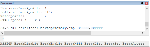
For the first point, the Keil debugging documentation includes the “SAVE” command, that seems to be what we need for this operation (“The SAVE command writes a memory image range to a file using the HEX386 format”)
For the second point, we need to look at the microcontroller’s datasheet, that should include this information:
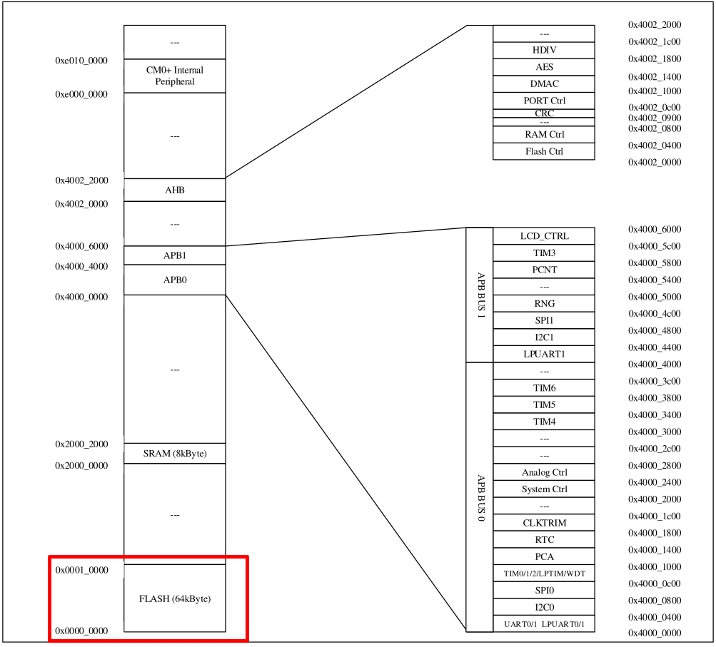
The flash memory starts at address 0x0 and ends at address 0xFFFF (next memory region starts at 0x1000). So, we can dump this memory location with the command “SAVE <OUTPUT_PATH\OUTPUT_NAME> 0x0000,0xFFFF”:
We can load our memory dump using our favorite disassembler. I will use Ghidra because it is free and supports the current architecture. Our dump can be loaded in Ghidra with the following configurations:
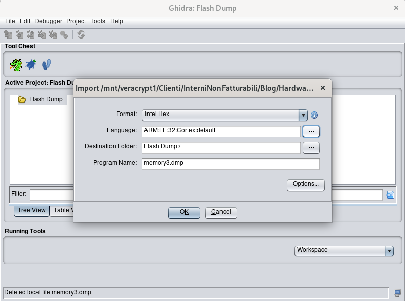
As stated in the Keil “SAVE” command documentation, it saves the dump in HEX format. From the microcontroller datasheet we know that the processor is a 32bit ARM Cortex, little endian.
After loading the binary, Ghidra will ask to analyze it. Default analyzers are usually enough, but the “ARM Aggressive Instruction Finder (Prototype)” and the “Decompiler Parameter ID” can be added to try to improve the results of the analysis.
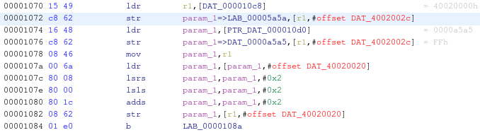
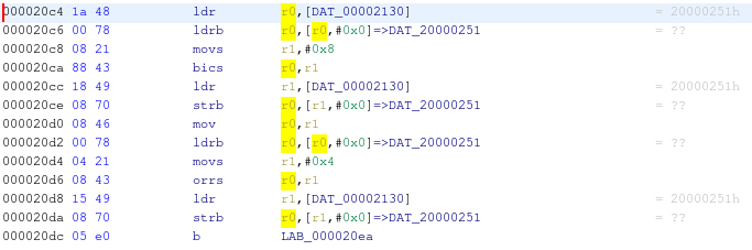
After the analysis, we can start to analyze ARM disassembled code and Ghidra pseudo-decompiled code. One thing that immediately catches the eye is the presence of many references to unresolved memory addresses. The following screenshot shows some examples that reference addresses 0x20000XXX and 0x400200XX (in red):

The reason of this unresolved memory address is that we loaded into Ghidra only one portion of the memory map of the microcontroller, but the memory map we saw in the datasheet included many other sections:
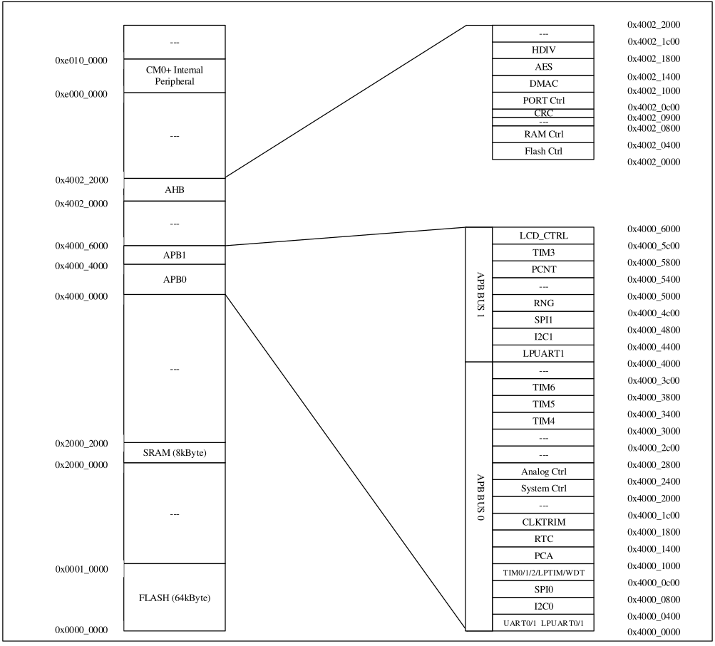
Some memory sections refer to actual SRAM memory, while others refer to memory-mapped peripherals (peripherals that can be used by reading/writing specific addresses in memory). These memory sections are important to understand how the code interacts with the chip peripherals and features. As we can see in the memory map, references to 0x20000XXX relate to the SRAM memory region and 0x40020XXX to AHB (Advanced High-performance Bus, a bus protocol introduced by ARM Ltd company). Other sections present are the two APB sections (Advanced Peripheral Bus, another ARM bus protocol) and one for the internal peripherals.
In order to make the code more readable, we can add these memory sections to Ghidra. We can do this operation quite quickly if we only add the five macro-areas on the left (SRAM, APB0, APB1, AHB, CM0+ Internal Periphericals) but the resulting disassembled code will be less precise. Adding the detailed memory sections on the right can produce better results, but it will be more time-consuming. Leveldown Security released a Ghidra plugin named SVD-Loader that could speed up this process. This plugin not only does add the memory regions but also the data structures used in the communications to the peripheral. Unfortunately, I could not try this plugin (I will explain the reasons shortly) but if it works it could greatly improve the analysis and consequently it is worth mentioning.
The Keil documentation offers the following definition of the SVD files: “The CMSIS System View Description format(CMSIS-SVD) formalizes the description of the system contained in Arm Cortex-M processor-based microcontrollers, in particular, the memory mapped registers of peripherals. The detail contained in system view descriptions is comparable to the data in device reference manuals. The information ranges from high level functional descriptions of a peripheral all the way down to the definition and purpose of an individual bit field in a memory mapped register. CMSIS-SVD files are developed and maintained by silicon vendors.”
The point is that SVD files are included in many Keil pack files (the files published by the vendors to allow Keil to interface with their modules). With this file, using the mentioned Ghidra plugin, we should be able to add memory sections and structures to Ghidra automatically. Pack files can be retrieved from Keil’s website (they can be hosted directly on the Keil website or linked). After downloading a pack file (that is a ZIP archive), we can extract its content and search for an SVD folder. If the folder is present, it may contains two types of file: XML files with .svd extension and binary files with .sfr extension. The binary files with the .sfr files (peripheral register files) are generated from the XML files after their validation from a Keil component named SVDConv (System View Description Converter). If we are lucky and the vendor released the XML SVD files, we can try to use the Ghidra plugin SVD-Loader. Unfortunately, we were not so lucky and HDSC released only the sfr files. Probably it is not difficult to convert back the sfr files to the XML SVD original format (online there are some Python implementations of the SVDConv utility) but for now I will simply manually add to Ghidra the memory sections I’m interested in.
We can add memory regions to Ghidra from the “Memory Map” tool present in the “Window” menu:
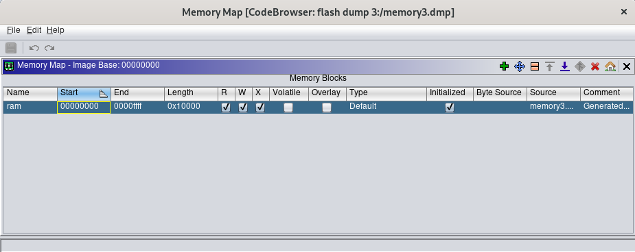
Initially, it contains only the memory block with the flash content (that Ghidra named “ram”). We can rename it to “flash” for convenience.
Then we can add new memory blocks using the “plus” icon on the right (in this example I will only add the two memory blocks mentioned earlier, addresses 0x20000XXX and 0x400200XX). Using the datasheet as a reference we can add the blocks “SRAM” and “Flash Ctrl”. One important thing: the data memory related to the peripherals should have set “Volatile” flag set. This results in the following memory map:
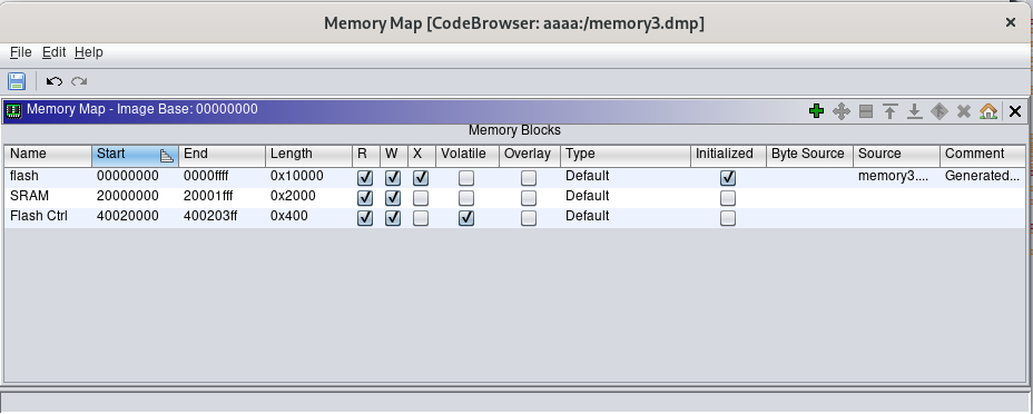
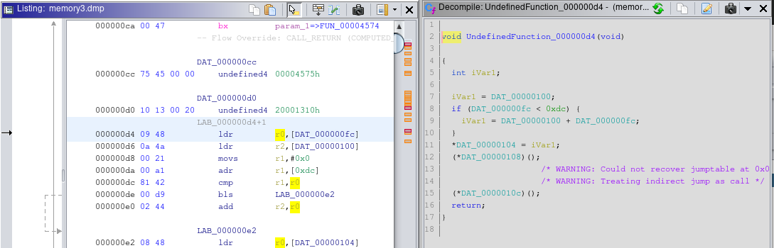
The result unfortunately is not the same as using the SVD-Loader Ghidra plugin (that loads also the data structure used by the peripheral), but setting correctly the memory regions (with the volatile flag set) should improve the quality of Ghidra decompilation and disassembly. After setting the memory map, the red addresses (unresolved) are now fixed:
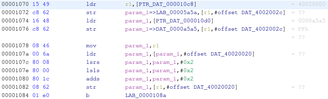
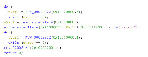
The decompiled code is also more readable when read/write operations are executed on the peripherals memory regions marked as “volatile” (in this example 0x40000000):
Last but not least, when we attached the SWD debugger, our target device reset and paused at the first instruction (address 0xD4). If we go to that address with Ghidra (‘G’ is the shortcut for “Goto”), we find an instruction inside an undefined function.
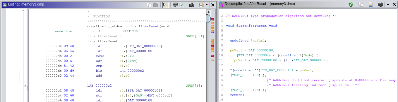
We can create a new function at 0xD4 address with the ‘F’ shortcut, in order to name the code that is executed after the reset of the device. After creating a function we can rename it with the ‘L’ shortcut (I named it “firstAfterReset”). The result is the following:
We are now able to analyze the firmware of the device. We will continue our analysis in the next post.
Cheers!