Intro
A few months ago, I read the work of Jeroen Delvaux, Cristofaro Mune, Mario Romero, and Niek Timmers on bypassing Secure Boot on an ESP32 V3 chip with both Secure Boot and Flash Encryption enabled. Their research demonstrated how it was possible to modify the flash memory to obtain an arbitrary CRC value, which would then be used through a single glitch (through EMFI) to execute arbitrary code.
I found this research particularly interesting because it was not the typical “glitch and pray” (© Raelize) fault injection, but rather a well-thought-out approach that leverages a chain of issues to reach a specific goal. It clearly demonstrated that fault injection is increasingly becoming a viable and practical attack vector – not just about escaping a single instruction, but involving much more complex scenarios.
The presentation and paper are available here:
- https://www.usenix.org/system/files/woot24-delvaux.pdf
- https://www.usenix.org/system/files/woot24_slides-delvaux.pdf
- https://www.youtube.com/watch?v=vx_j0L7xL8Y
The main goal of my research, documented in this article, is to verify whether the attack could also be performed using voltage injection, and to explore possible ways to improve on it.
Please note that in order to fully understand this article, it is important to have read the research mentioned above. Reading my earlier blog posts on hardware fault injection is also recommended, as many points I make here may otherwise be unclear.
Environment setup
To replicate the attack, I relied on a custom ESP32 board that is normally provided during the TAoFI training, and for which schematics and data are available here. Unlike the original board that uses an ESP32-D0WDQ6 processor, I mounted an ESP32-D0WDQ6-V3, which includes many security patches following various demonstrated attacks over the years.
For all experiments, I used the Chipwhisperer Husky, performing glitching on VDD_CPU and VDD_RTC simultaneously. Naturally, for this test, I did not completely “shield” the processor enabling all security features, so I could work on it comfortably. However, everything is feasible even with a processor with all security features enabled.
I set up the processor with Secure Boot and Flash Encryption using custom keys.
# Generate signing keys and burn them on the ESP32
espsecure.py generate_signing_key --version 2 secure_boot_signing_key.pem
espefuse.py -p /dev/ttyUSB1 burn_key_digest secure_boot_signing_key.pem --show-sensitive-info

# Enable Secure Boot protection on boot
espefuse.py  -p /dev/ttyUSB1 burn_efuse ABS_DONE_1 1

# Generate encryption keys and burn them on the ESP32
espsecure.py generate_flash_encryption_key aes.bin
espefuse.py -p /dev/ttyUSB1 burn_key flash_encryption aes.bin --show-sensitive-info

# Enable Flash Encryption
espefuse.py  -p /dev/ttyUSB1 burn_efuse FLASH_CRYPT_CNT 1
espefuse.py  -p /dev/ttyUSB1 burn_efuse FLASH_CRYPT_CONFIG 15
Solving equations…
The first part of the attack involved having a specific CRC32 on the verification signature data in the secure boot. This is necessary as a starting point to then cause a glitch that can perform operations in a controlled manner, specifically a jump to the desired address. However, the signature data is also encrypted in the flash, so achieving an arbitrary CRC32 calculated based on the plaintext is not at all a trivial task. The original article highlights how this is possible because there is an information leakage in the ROM. If the calculated CRC32 does not match the stored one, an error message is printed that contains both CRC32 values.
I have to admit that when I first read the paper, I completely skipped over Chapter 3.3 Solving Equations… It’s been quite a few years since I finished University, and I’ve never really been a big fan of math since then. I know it, I use it – but only within a limited scope. The paper presents two different methods to achieve the goal of obtaining an arbitrary CRC32 by working on encrypted data: one based on a brute force attack and the other on the possibility of solving a system of equations.
For the first tests, I “cheated” a bit: I modified the firmware in plaintext and then performed the flashing process, which would take care of encrypting it. But then I asked myself —is it really that complicated to try and follow the full process to perform a complete attack? I didn’t want to waste too much time, so I wrote some code that “emulates” the flash decryption process and CRC32 calculation. The code is almost identical to what’s used in espsecure.py, and it was taken from here:
The goal was simply to speed up the various tests I performed, without the need to have an ESP32 physically available or to arbitrarily modify the flash. I downloaded the first part of the flash, which includes several components — most importantly, the bootloader and the signature. In my case, the bootloader starts at address 0x1000, and the signature section is located at 0xD000.
esptool.py --chip esp32 read_flash 0x0 0x10000 signature_block.bin
Of course, on a fully protected chip, this operation should be performed by directly reading the external flash chip, rather than accessing it via bootloader mode but I’m quite lazy…
We can also inspect the contents of the dumped flash using the following command:
espsecure.py decrypt_flash_data --key aes.bin --address 0x0 signature_block.bin -o signature_block.bin_decrypted
At this point, I ran a few tests, but the results were not very satisfying — and I didn’t want to spend too much time on this topic…

Lately, I’ve been experimenting with using LLMs for various topics, with very mixed results — so I decided to give it a try on this one as well…
At this point, I asked an LLM to carefully analyze the PDF containing the details of the attack, focusing on the chapter related to methods for achieving an arbitrary CRC32. I provided it with the previously created example code that simulates the encryption and decryption of memory and asked it to implement the attack. Naturally, I had to specify some details carefully, such as which blocks to work on, because the LLM itself was not able to correctly extract all needed information from the paper.
It was not a simple process; the generated code often did not work, and I had to correct many things before arriving at something functional.
We (me and the LLM) first focused on matrix invertibility, which led to the script crc32_matrix.py. It works well and, most importantly, produces results almost instantly while requiring only a minimal amount of leaked information. Generally, to achieve our objective on a real target, we would need to modify the flash 40 times and then associate the modification with the calculated CRC32 result to have all the necessary data for the final calculation.
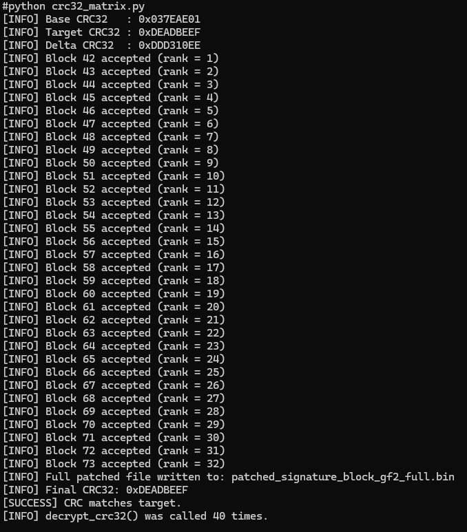
At this point, I attempted to write the patched firmware directly onto the ESP32.
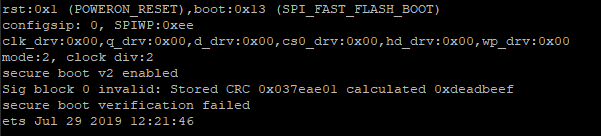
esptool.py --chip esp32 --port=/dev/ttyUSB1 --before=default_reset --after=no_reset write_flash --flash_mode dio --flash_freq 40m --flash_size keep 0x00 patched_signature_block_gf2_full.bin --force
And indeed, the result was perfect.
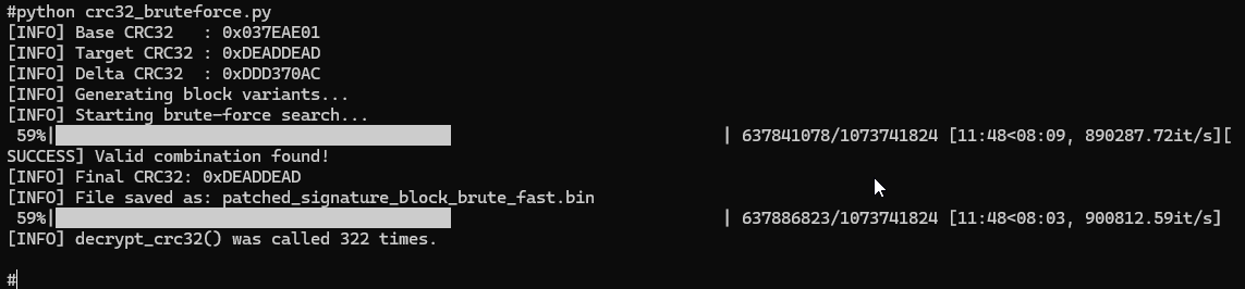
For sake of completeness, I also tried switching to a brute-force approach to achieve a result in case the previous method didn’t work properly. After some tuning of the variables, I obtained a good outcome also with this method. It typically takes around 10 to 15 minutes to produce a valid result while limiting the flash modifications to about 330. The code is available here: crc32_bruteforce.py
Let’s try it on the ESP32 in this case as well.
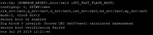
esptool.py --chip esp32 --port=/dev/ttyUSB1 --before=default_reset --after=no_reset write_flash --flash_mode dio --flash_freq 40m --flash_size keep 0x00 patched_signature_block_brute_fast.bin --force
And everything appears to be working correctly.
I have to admit that, since this wasn’t my main focus, I probably would have skipped this part entirely if it weren’t for the help of an LLM…
Trying the voltage glitching
Now that we have an arbitrary value in one of the registers thanks to CRC32, the paper suggests using a glitch to “jump” through a JMP or CALL instruction to the address previously calculated by CRC32. Starting from the information provided in the paper, we know that the code we’re interested in will be executed immediately after the different memory regions are read from flash. These regions are summarized below.
Using an oscilloscope with the trigger on the reset signal and one channel on the flash’s chip select line, I identified that the flash reading phase ends approximately 38.5 milliseconds after power-up using my setup.
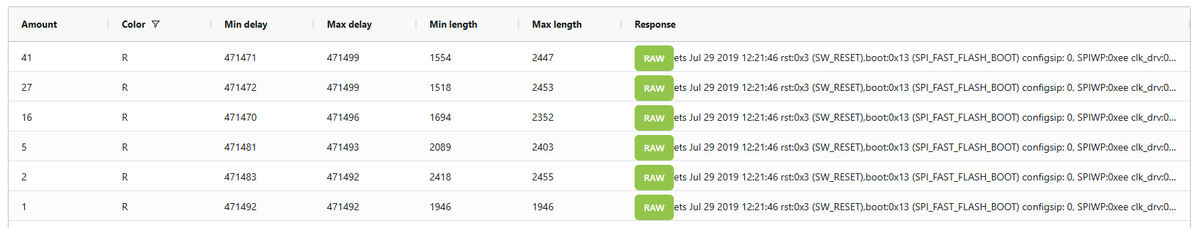
For the rest of the testing, I followed the same approach as described in the paper—using the CRC value at address 0x80006864 as a reliable feedback mechanism by triggering a call to the ets_fatal_exception_handler function which prints on the serial line.
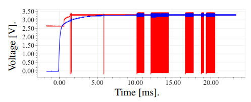
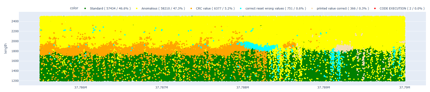
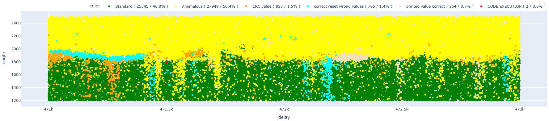
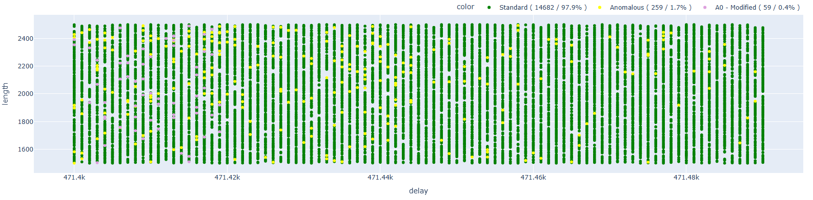
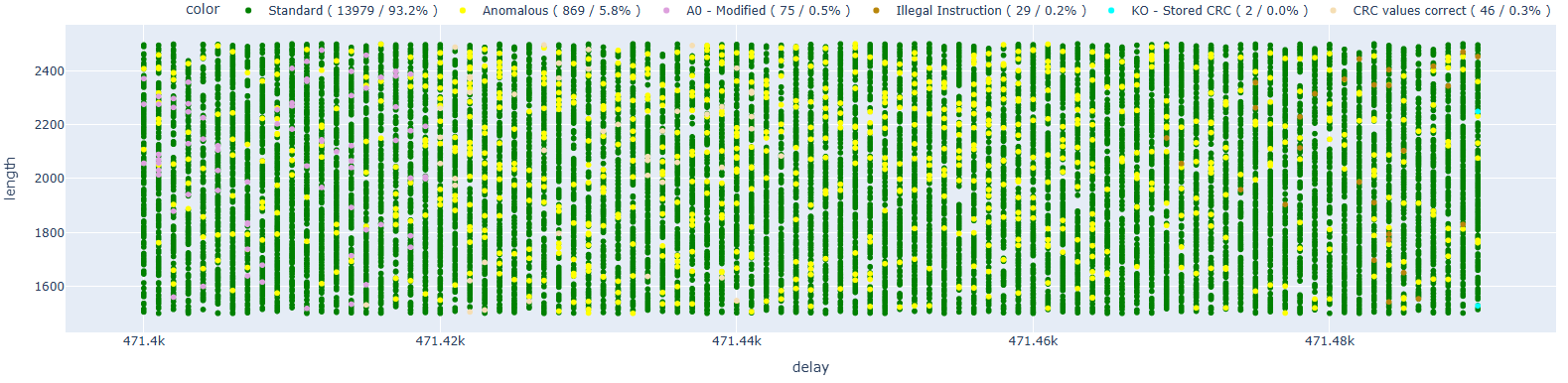
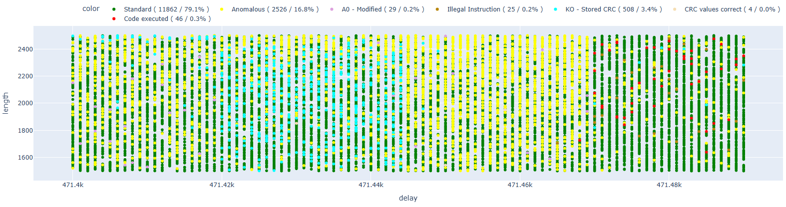
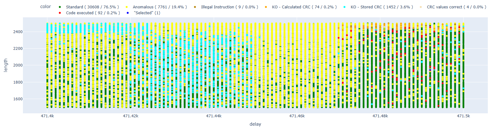
At this point, I launched the attack, hoping to obtain some valid results. As in the paper, I classified the outcomes to distinguish cases where I affected the CRC functions from those where it was already too late in the execution flow.
After several tests, I achieved the first code execution (highlighted in red in the following chart)! I also categorized other types of results to provide additional context; however, for this initial phase, the only thing that mattered was determining whether the attack was feasible or not.
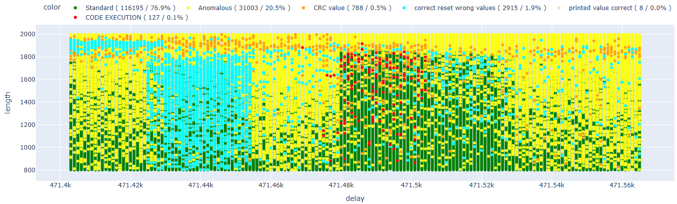
Let’s now try to narrow down the range to a more appropriate window.
Now that we know for sure the attack is feasible, let’s see if we can significantly improve the success rate.
The importance of the right trigger
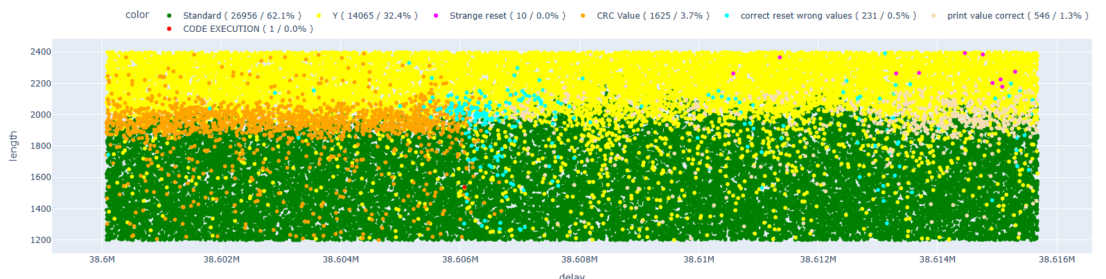
During the TAoFI training (which I highly recommend), we were shown how important it is to have a clean trigger signal that allows us to work with precise and stable timing. Up until now, we’ve been using the reset signal as the trigger, which is not ideal.
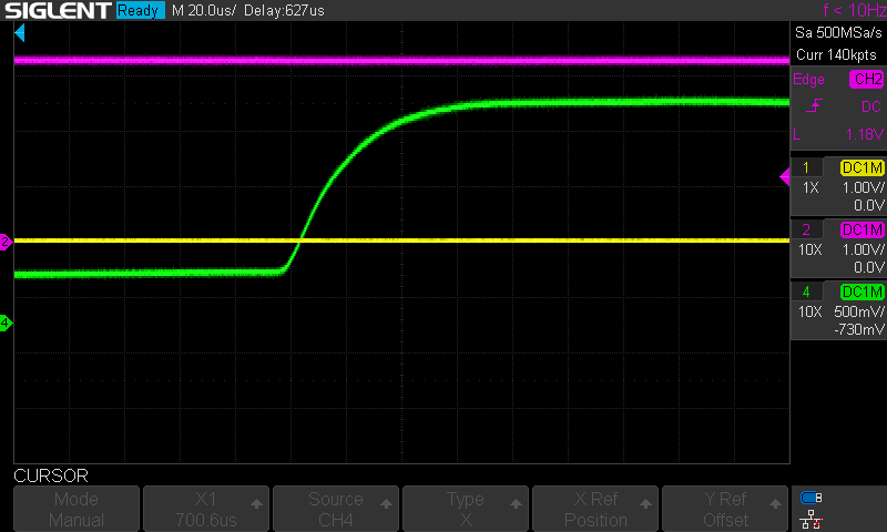
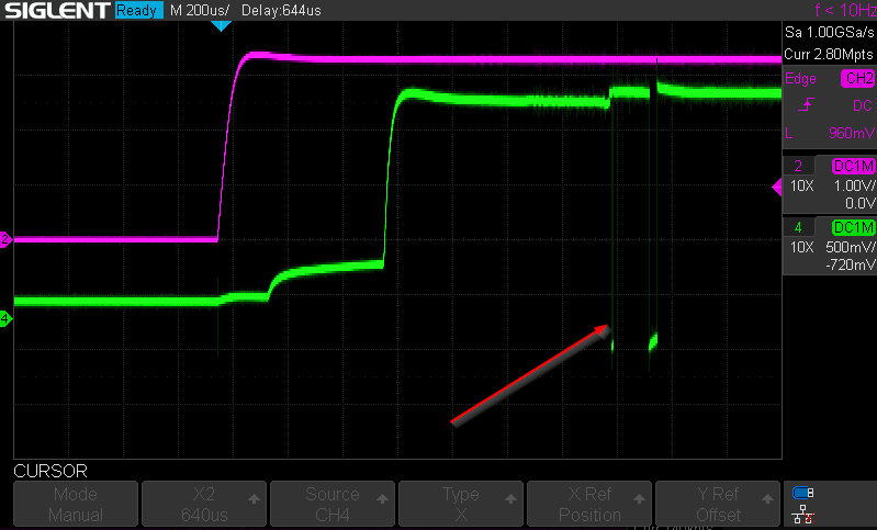
Through some tests with the oscilloscope, I observed that using this method often results in glitches that vary significantly from one attempt to another. In this image, for example, we can see the reset signal in purple and the chip select line in green.

If we zoom in on the waveform, we can clearly see that during the power-up phase, the CS (chip select) signal also transitions from 0 to 3.3V over a relatively long period of time—and. This behaviour often varies from one boot to another.
For this reason, using these signals as the initial trigger was not optimal.
However, if we look at the subsequent CS change of state, we can see that they are significantly faster and more consistent compared to the initial one.
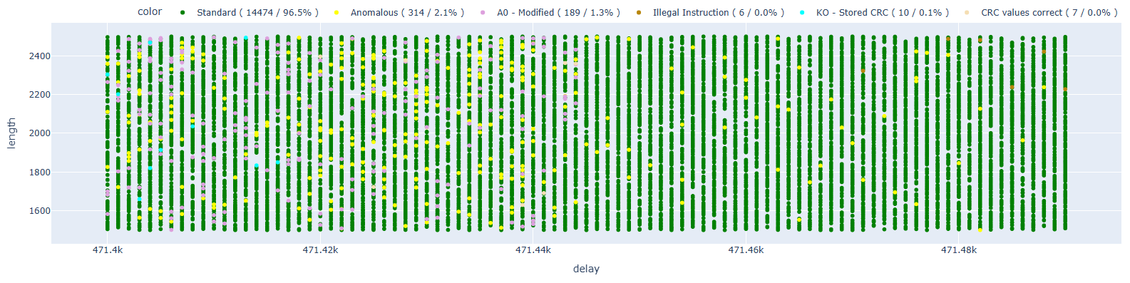
At this point, I decided to run the same attack, but this time using a specific feature of the ChipWhisperer Husky that allows for an advanced trigger. This feature enables us to count a defined number of rising/falling edges before firing the actual trigger.
cw_scope.adc.basic_mode   = 'rising_edge'
cw_scope.trigger.module   = 'edge_counter'
cw_scope.trigger.triggers = 'tio4'
cw_scope.trigger.edges     = 3
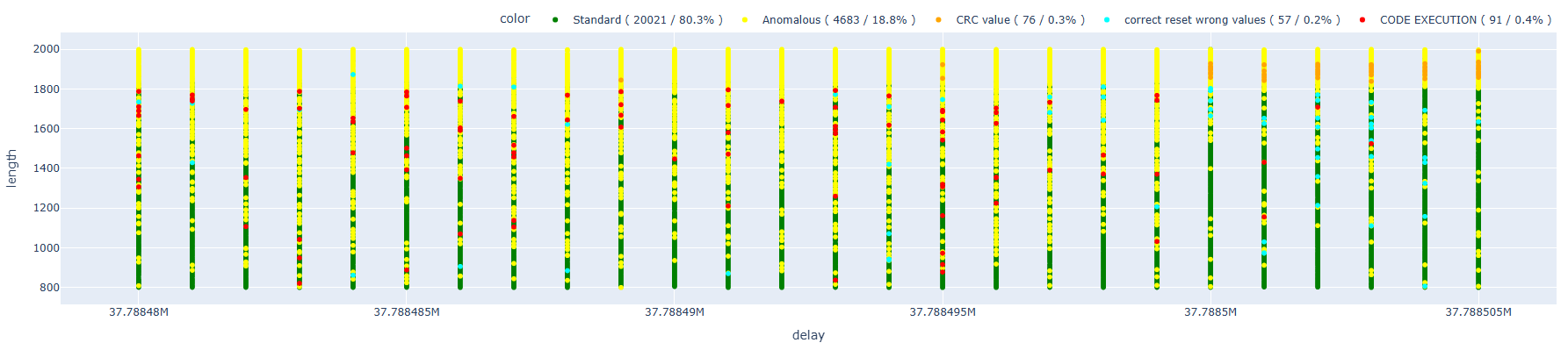
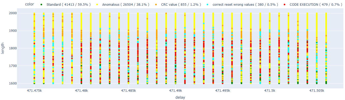
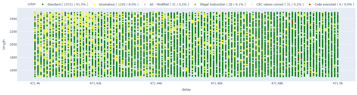
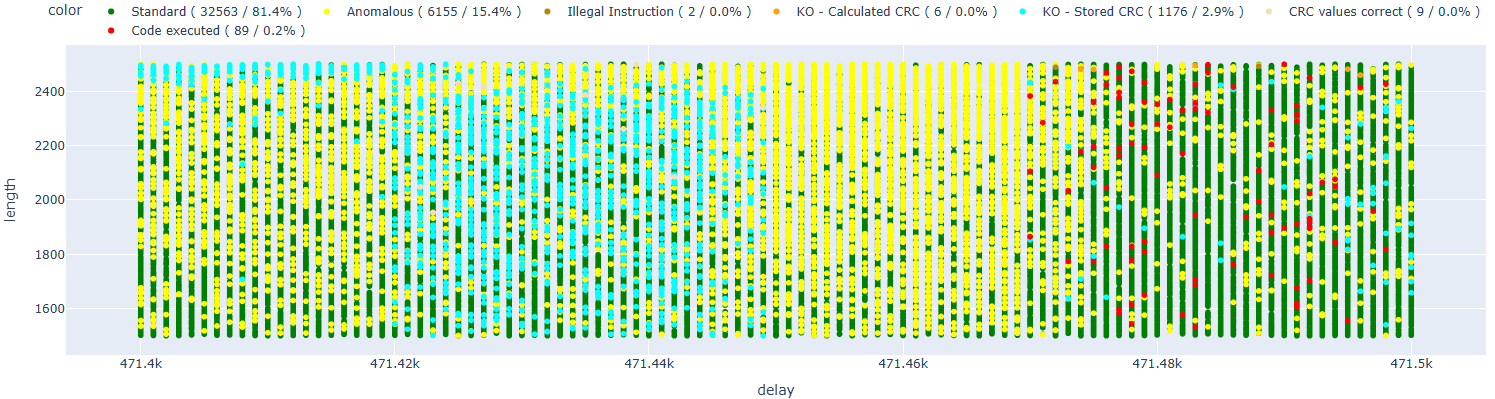
Now we need to readjust the new delays relative to the previous setup, and we’ve obtained the following results.
If we compare this image with the previous ones, we can immediately see that some elements are more “defined” and less scattered – the patterns appear much more precise.
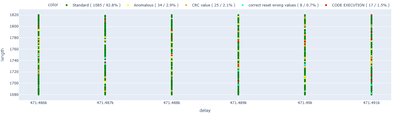
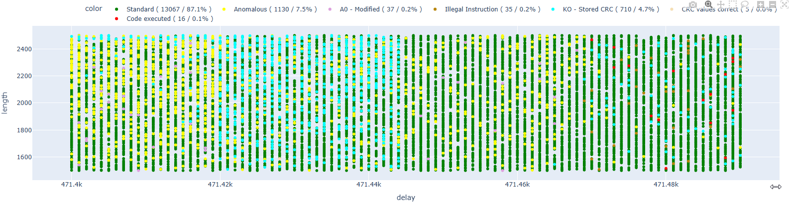
Let’s now try running a test within the area of interest.

As we can see, the faults that lead to code execution are concentrated in two distinct areas. We can hypothesize that these correspond to the two possible solutions proposed in the paper (one in crc32_le and the other in the ets_secure_boot_verify_signature function).
By narrowing down the areas of interest, I was able to achieve successful results with a hit rate of approximately 0.4%.
Let’s now consider what happens from a logical perspective. We’re introducing a glitch after a delay of approximately 37.7 milliseconds, which — given that the processor is running at 80 MHz at this stage — translates to roughly 3,016,000 clock cycles. However, we’re not accounting for the fact that some memory read operations might be delayed or repeated due to transient faults or retries. For this reason, it’s crucial to trigger as close as possible to the injection point, in order to minimize error margins and improve timing accuracy.
At this stage, we can try switching to a closer edge counter. Ideally, we would want to start counting edges from the last memory block, but unfortunately, the CW Husky does not support this kind of trigger alignment.
What we can do instead is start counting edges from the very beginning. However, we’ve observed that the number of edges sometimes varies from one execution to another, so we cannot reliably base our trigger on the last one. This also helps us understand that we’ll inevitably be working with noisy values.
After various tests, I managed to identify some values that work well in this case:
cw_scope.adc.basic_mode   = 'rising_edge'
cw_scope.trigger.module   = 'edge_counter'
cw_scope.trigger.triggers = 'tio4'
cw_scope.trigger.edges     = 3337
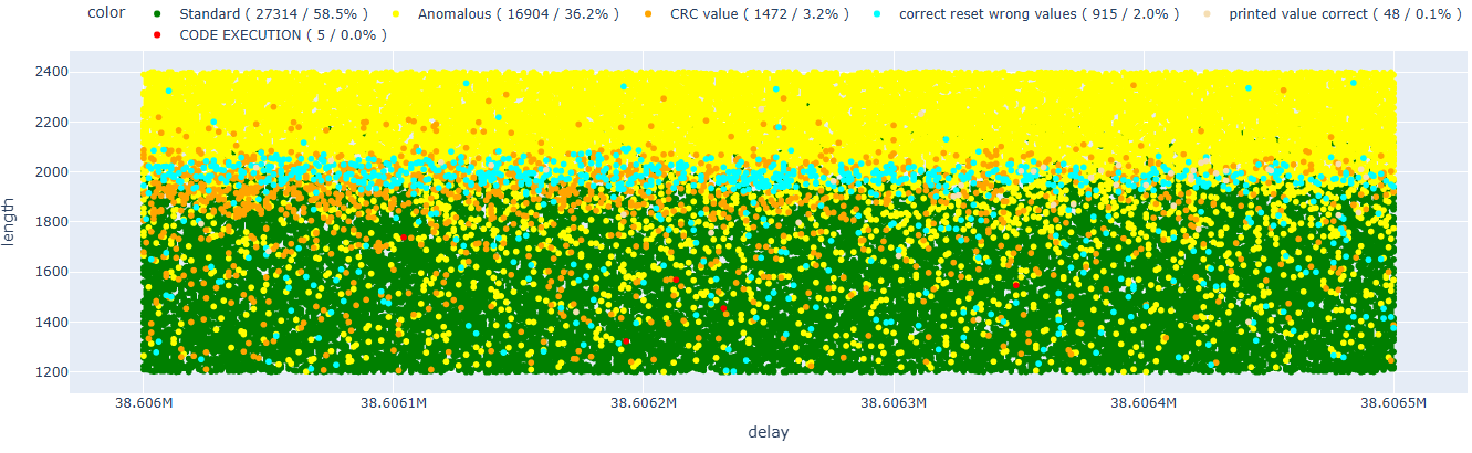
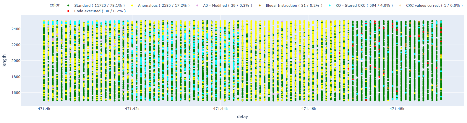
As we can see, we went from a delay of approximately 37.7 ms down to just 0.47 ms, bringing us significantly closer to the injection point.
This is clearly reflected in the graph below, where the results appear even cleaner and more defined compared to previous attempts.
At this point, we can focus our efforts on the two previously identified areas.
From the graph, we can see that the first area has completely disappeared. This is most likely due to errors caused by long delays. Based on the data we currently have, we cannot be certain whether these faults refer to one or more possible faults that were proposed in the paper.
We can also focus on a more specific area.
After various tests limiting the area of interest, I managed to reach a 1.5% success rate.
Having a precise and “close” trigger to the point of interest allows for much more accurate glitches and, consequently, a better success rate.
“Oh dear! Oh dear! I shall be too late!” – And so Alice followed the White Rabbit…
One of the most impactful aspects for me is the fact that these attacks are generally labeled as non-deterministic. So, when I first started, I was facing a huge search space without even knowing whether the attack was feasible in my specific conditions — in fact, the original attack had been performed using EMFI glitching.
During the first few days of testing, I wasn’t successful. I had no idea if I was glitching in the right window, or whether it would ever work at all. So I asked myself: Isn’t there a better way to understand where the glitch should be applied?
Let’s break down the context:
- We’re inside the ROM, running a bootloader verification routine. No exception handlers are set — so either we get some UART output or the processor simply reboots.
- We’re in a controlled test environment, on a dev board.
- On the Xtensa architecture, there’s no equivalent to ARM TRACE.
So… what if we tried to leverage JTAG to help us?
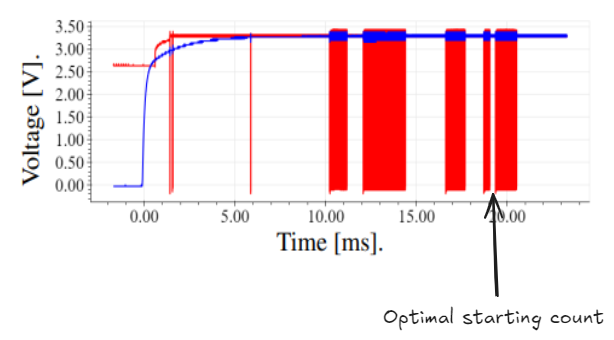
At this point, I set up JTAG with an active GDB server. In my case, I found that I had to increase the supplied voltage for everything to work correctly — otherwise, I encountered inconsistent errors and incorrect CRC32 calculations.
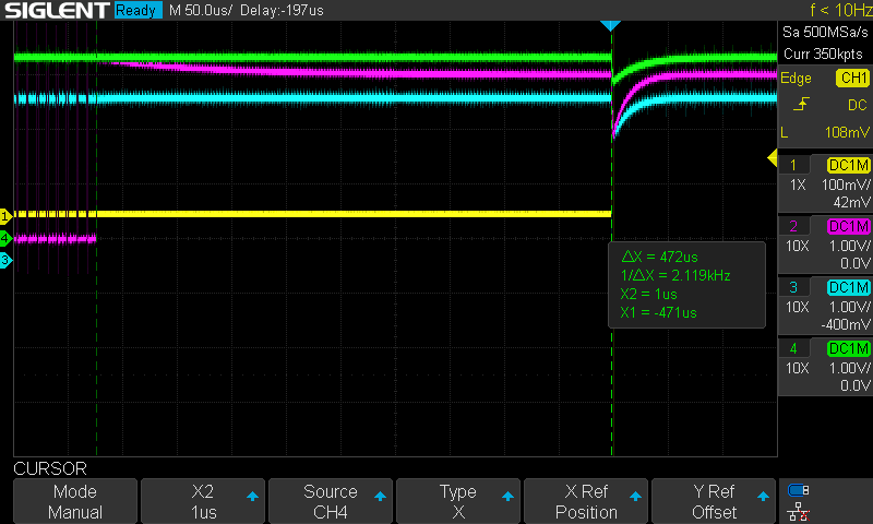
The idea is based on the fact that if I apply a glitch with a length above a certain threshold, the processor either reboots or hits a specific error. The goal is to use GDB to set a hardware breakpoint at the instruction we want to glitch.
- If GDB hits the breakpoint, it means we waited too long.
- If the processor reboots, it means we glitched too early.
This forms the basis for a standard binary search strategy, allowing us to pinpoint the exact moment when the instruction was executed.
The flow can be summarized as follows (where Z is an arbitrary range):
To use GDB directly from Python scripts, I used the pygdbmi library, which allows to send commands directly to GDB and read the results. It is certainly not the optimal method, but it is the fastest one.
This method doesn’t give us the exact value, but it allows to quickly narrow down the range where we should be working. The code is available here: gdb_search_space.py.
I have to say, it doesn’t always work perfectly and requires some parameter tuning. I used it on the ESP32 at 3.15V with a glitch length of 5000ns. My recommendation is to find a glitch length that consistently triggers an “Illegal Instruction” exception, so that you have a clean and predictable response.
Also keep in mind that the script puts the processor into a predefined state after a soft reset, so some things won’t happen in this setup — for example, in our case, one edge count is missing.
At this point, I ran it over a very large range, simulating our initial blind attempts. Using a delay range from 1 to 50.5 million, it found that the instruction of interest we focused on was executed at a specific point and managed to identify the point in just 23 attempts. This identifies the area where we need to perform the glitching, and it is the same one we had found previously after days of testing!

Even though not very precisely, I took a screenshot of the oscilloscope to compare it with future runs.
Same procedure repeated using the edge counter we’ve been working with so far, set to 3336.

In this case as well, I took a screenshot from the oscilloscope. I didn’t move the cursors, and we’re roughly at the same point again.
Compared to the script I was using with a 1.5% success rate… it’s pretty much the same.
During testing, I noticed that sometimes GDB gets a bit messy, and in some cases the parameters don’t provide a clear picture — there’s definitely still some work to be done. The script doesn’t give you the exact point, but it’s an excellent start.
“Would you tell me, please, which way I ought to go from here?” – Alice
At this point, I asked myself: If GDB works so well for finding the injection point, why not use it to understand what’s actually happening? Let’s give it a try…
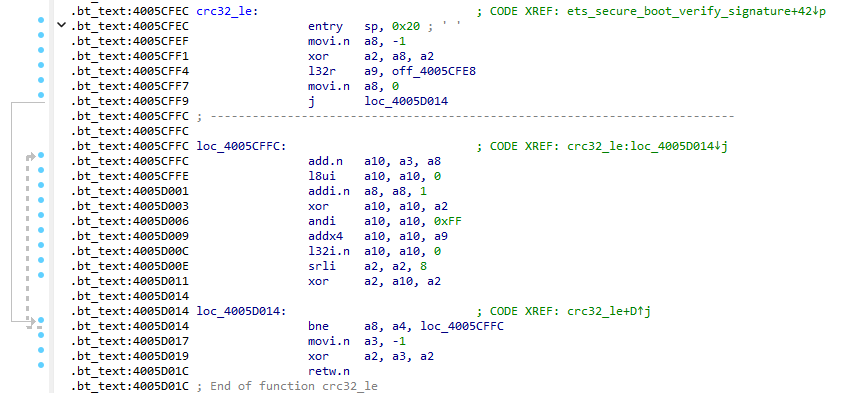
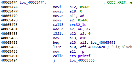
The paper initially hypothesized two possible locations where code execution might occur: the first by corrupting address 0x4005D019, and the second at 0x40065485.
For completeness, I am providing the code below that we will work on.
The first approach I tried was to use GDB exactly as I did when identifying the injection point.
If I set a breakpoint at address X, and it always hits – and I never observe execution of our code — then it’s very likely that code execution occurs due to a fault in that instruction or one of the subsequent ones. This can allow to effectively identify the injection point that enables us to have control over the PC as we desire, and consequently achieve code execution.
As a first attempt, I ran some tests by setting a breakpoint at address 0x4005D019, the first location hypothesized as responsible for the modification of register A0.
My expectation was that no code execution would occur at this point, since halting execution with GDB would almost certainly interrupt the normal flow of the target instruction’s execution.
Analyzing the results, we can see how A0 (that is, the return address that will be executed after the RET instruction) has been modified multiple times (I only report the main results), in particular:
- 48 times – 0x800658d9
- 7 times – 0x3ff40000
- 4 times – 0x4ac
Let’s move on to the second attempt, setting the breakpoint at address 0x4005d01c, which is right on the RET instruction.
With the same number of samples, we immediately see how the number of results with A0 modified is significantly higher (189 vs 59), and especially, it is possible to see that there is a new area in terms of delay that was not there before. We can therefore hypothesize that this entire area is caused precisely by the fault on instruction 0x4005d019, which shifts different values into A0. In this case, A0 had the following values (I only report the main results):
- 111 times – 0x800658d9
- 17 times – 0x8000fab6
- 13 times – 0x40000740
- 5 times – 0x4ac
- 2 times – 0x3ff40000
Let’s now move to the next address, 0x40065481, which should be the first of the ets_secure_boot_verify_signature function that runs after the crc32_le function.
In this case, we also do not have any code execution. The previous result, together with this one, allows us to assert with a certain degree of confidence that the instruction 0x4005d019 is not as easily modifiable as we would like.
Let’s now try with the breakpoint at address 0x40065483.
In this case, we have instances of code execution, which allows us to hypothesize that fault injection happened earlier.
Let’s now move on to instruction 0x40065485.
Here we have some instances of code execution, so the fault injection definitely occurs earlier.
Let’s move on to the next instruction, at address 0x40065488.
In this case, we also have some instances of code execution, which seem to double compared to the previous test.
Let’s move on to the next instruction, at address 0x40065491.
Here we also see how the number of code executions continue to increase compared to the previous attempts; this could be an error caused by the use of GDB or the fact that more instructions allow us to achieve the same result.
In Delvaux’s article, a comparison of the registers was made using the result of stdout, but we have an active GDB session…
The normal operation of that piece of code is as follows (red values are registries that change):
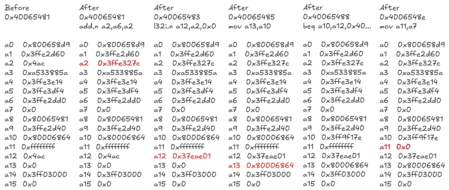
It is important to remember that, as explained in my previous articles, there is a possibility that glitching may affect multiple instructions.
Let’s now try to set a breakpoint at address 0x800068e4, which is precisely where we should jump in case of correct code execution, and compare the results of all the CPU registers to truly understand what is happening.
We have 6 different results; the following table summarizes the data for the identical results (i.e., those with the same records).
Some considerations on all the results:
- A0 (the return address) is correct, so it is unlikely that we are inside another function, such as print, and it is unlikely that we have excuted a call instruction
- A11 is 0xfffff, so it is before the last instruction (0x4006548e)
The state of the different registers is summarized as follows:
Case 1:
a12 0x0         -> 0x40065483 not executed correctly (but executed)
a13 0x80006cec  -> 0x40065485 not executed correctly (but executed)

Case 2:
a12 0x0         -> 0x40065483 not executed correctly (but executed)
a13 0x80006864  -> 0x40065485 executed correcly

Case 3:
a12 0x37eae01   -> 0x40065483 executed correcly
a13 0x80006864  -> 0x40065485 executed correcly

Case 4:
a12 0x0         -> 0x40065483 not executed correctly
a13 0x0         -> 0x40065485 not executed correctly or not executed

Case 5:
a12 0x0         -> 0x40065483 not executed correctly (but executed)
a13 0x800068ec  -> 0x40065485 not executed correctly (but executed)

Case 6:
a12 0x0         -> 0x40065483 not executed correctly (but executed)
a13 0x800068e4  -> 0x40065485 executed correcly
The presence of these instructions gives us some confidence in stating that the fault occurs at or past instruction 0x40065488. However, this contradicts what we observed earlier, as in previous tests with the breakpoint set at address 0x40065483, we encountered the first faults. These conflicting results might indicate that:
- The hardware breakpoints could be affected by glitching.
- The hardware breakpoint might not have been triggered correctly in some cases.
This is certainly an area that needs further exploration. So, which instructions allow us to jump to our address correctly? We do not know for sure, but the evidence suggests it is either one of the following instructions:
0x40065488 beq a10,a12,0x40065498
0x4006548b l32r a10,0x40065428
Until now, we have used 0x800068e4 as the calculated CRC. Let’s try the same experiment with 0x400068e4 to see if there might be any differences.
In this case as well, the results are very similar to the previous ones, and we have similar cases.
Case 1
a12 0x0
a13 0x40006cec

Case 2
a12 0x37eae01
a13 0x40006864

Case 3
a12 0x0
a13 0x40006864

Case 4
a12 0x0
a13 0x0

Case 5
a12 0x0
a13 0x400068ec

Case 6
a12 0x0
a13 0x400068e4
Conclusions
This work started as a curiosity-driven experiment to replicate and possibly improve on the attack presented by Delvaux et al. — but quickly turned into a deeper exploration of what it really takes to make fault injection reliable on a hardened target like the ESP32 V3.
While the original attack was carried out using EMFI, I demonstrated that voltage glitching can also be a valid and effective technique. The key enablers were:
- The use of advanced trigger strategies, especially through edge counting
- A GDB-assisted binary search approach to narrow down injection points
- And, surprisingly, the help of an LLM to accelerate testing and code development
Despite some early failures, iteratively refining the approach (both in terms of trigger alignment and fault targeting) allowed me to push the success rate up to ~1.5%, which is a solid starting point for future optimizations.
More importantly, this experience suggests that — when the right tooling and methodology are in place — fault injection attacks are increasingly approachable, reproducible, and even automatable. Which is great for researchers, but not so great for defenders.
Furthermore, the use of JTAG with GDB has proven to be an excellent tool for identifying both the timing for executing a glitch and for analyzing the results.
There’s still room to improve: more precise delay tuning, better glitch characterization, and tighter integration with the CPU’s debug features could yield even better results. But the bottom line is clear: Voltage glitching on a Secure Boot + Flash Encryption-enabled ESP32 V3 is not only possible — it’s practical.