Intro
This series of articles describes fault injection attack techniques in order to understand their real potential by testing their limits and applicability with limited hardware (available on the market at an acceptable cost). It explores possible ways of using an attack that, in my opinion, is greatly underestimated.
First of all, I want to thank @pulsoid and @tieknimmers for their excellent Fault inject advanced course (TAoFI – The Art of Fault Injection) that I attended. In their training, they provide great insights and ideas, thanks to their pioneering work and passionate pursuit of these topics. One of the mantras of the course was “Don’t glitch and pray” (© Raelize), and I tried to internalize this concept as much as possible. These articles were born precisely from that.
The term glitching refers to an external behavior that causes a chip to enter an anomalous state, allowing for the creation of a fault, which is an internal error that enables the execution of something different from what was expected. Let’s start with the basics. There are four main techniques for performing fault injection on a chip:
- Voltage glitching
- Clock glitching
- Electromagnetic glitching
- Optical glitching (laser)
I will focus on the voltage glitching part, as it is one of the most approachable techniques with limited hardware. The basic concept is that we “deprive” the chip of power, making it “unstable”.
There are several ways to perform voltage glitching, primarily:
- Crowbar to ground (used by ChipWhisperer)
- Crowbar to high voltage (which risks burning the chip)
- Controlled VCC (by providing a controlled different voltage)
For now, we will use the crowbar to ground technique, which is used by ChipWhisperer devices. During the tests, I mainly used ChipWhisperer-Husky. A detailed description of the technique can be found at: https://eprint.iacr.org/2016/810.pdf
As for the target of these attacks, I have chosen to work on ESP32 for various reasons, primarily:
- There is already a lot of available material on attacks.
- There is a “patched” v3 chip that should solve multiple issues on which it will be possible to test the resistance of the countermeasures implemented.
- It was the chip used in the TaoFI course, so I already have a working board ready.
The main past works on these chips are the following (hoping to mention them all):
- Pwn the ESP32 Secure Boot https://limitedresults.com/2019/09/pwn-the-esp32-secure-boot/
- Pwn the ESP32 Forever: Flash Encryption and Sec. Boot Keys Extraction https://limitedresults.com/2019/11/pwn-the-esp32-forever-flash-encryption-and-sec-boot-keys-extraction/ + https://www.youtube.com/watch?v=vwwTC_ivG00
- Espressif ESP32: Bypassing Secure Boot using EMFI https://raelize.com/blog/espressif-systems-esp32-bypassing-sb-using-emfi/
- Espressif ESP32: Controlling PC during Secure Boot https://raelize.com/blog/espressif-systems-esp32-controlling-pc-during-sb/
- Espressif ESP32: Bypassing Flash Encryption (CVE-2020-15048) https://raelize.com/blog/espressif-systems-esp32-bypassing-flash-encryption/
- Espressif ESP32: Bypassing Encrypted Secure Boot (CVE-2020-13629) https://raelize.com/blog/espressif-esp32-bypassing-encrypted-secure-boot-cve-2020-13629/
- Unlimited Results: Breaking Firmware Encryption of ESP32-V3 https://eprint.iacr.org/2023/090.pdf + https://www.youtube.com/watch?v=wfZHQocTsZo
- Breaking the Flash Encryption Feature of Espressif’s Parts https://courk.cc/breaking-flash-encryption-of-espressif-parts
- Fault Injection Attacks against the ESP32-C3 and ESP32-C6 https://courk.cc/esp32-c3-c6-fault-injection
- Breaking Espressif’s ESP32 V3: Program Counter Control with Computed Values using Fault Injection https://www.usenix.org/conference/woot24/presentation/delvaux
I encourage you to read them to get familiar with the topic, otherwise you will likely struggle to understand the rest of this article.
Let’s start
Let’s now try to create a “clean” situation that allows us to better explore what happens with glitching.
Unlike many examples found online, our goal is not to skip an instruction but to understand what else can happen and why. Thus, trying to make a “world” considered non-deterministic a little more deterministic.
To do this, we need to:
- understand exactly which instruction(s) we are going to influence
- know the context (including other registers, memory areas, etc.)
So:
- we need to use as much ASM code as possible instead of C code in order to exclude unnecessary instructions (e.g., calls) that partially modify the context
- find a method to have a clear view of the context without influencing it
- use a limited number of instructions, especially ones that allow us to understand which one we are influencing
Preparation of the test environment
Using as few instructions as possible
Now let’s try to create an environment that is as clean as possible, and see how to improve the code that is normally used as a starting point.
Generally, when working on glitching examples, a trigger signal is used, which is when the code of our interest is executed. This helps us explore the data more precisely by narrowing down the scope.
This method is often used to change a trigger PIN:
GPIO_OUTPUT_SET(26,1);
However, if we look at how this is translated at the assembler level, it generates:

Essentially, the function “0x40009B24” (gpio_output_set) is called, which is present in the ROM. By disassembling the ROM, we can see what happens:
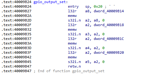
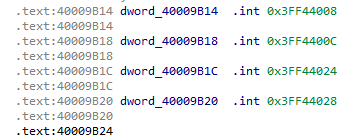
In the documentation, you can find details about the addresses used:

And, more specifically:
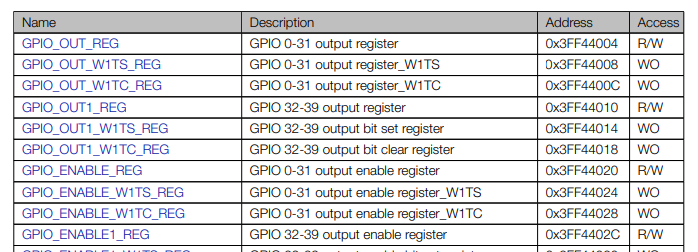
According to the reference manual, we can use GPIO_OUT_W1TS_REG to activate the pin and GPIO_OUT_W1TC_REG to deactivate it, thus eliminating a call and a series of unnecessary instructions that could cause problems during glitching.
The final assembler code will be:
// GPIO 26 PING HIGH using GPIO_OUT_W1TS
"movi a11, 0x4000000;"
"movi a12, 0x3ff44008;"
"s32i.n  a11, a12, 0;"

// GPIO 26 PIN LOW using GPIO_OUT_W1TC
"movi a12, 0x3ff4400C;"
"movi a11, 0x4000000;"
"s32i.n  a11, a12, 0;"
This way, we save instructions and tamper only with a very limited number of registers.
Having a clear understanding of the context
Once we have solved the initial problem, we need to find a simple way to maintain the context while losing as little information as possible.
My idea is to use CPU exceptions that allow to get a complete context (https://docs.espressif.com/projects/esp-idf/en/latest/esp32/api-guides/fatal-errors.html#illegal-instr-msg). The initial idea was to execute the code at the bootloader level to “speed up” the boot phase. However, the exceptions are directly handled by the ROM, and the classic “Guru meditation” has not been implemented yet:
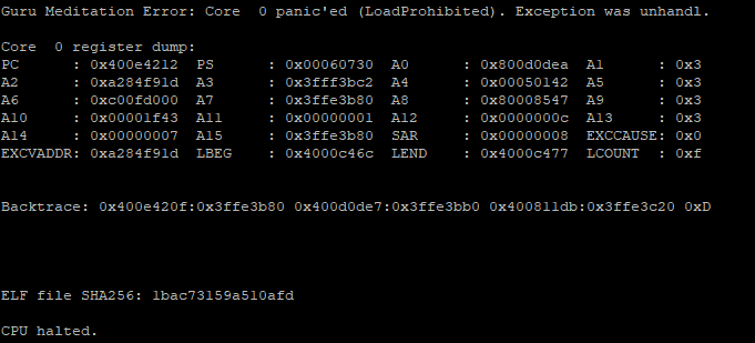
The advantage is having a complete context, but the downside is that each attempt would require resetting the CPU, resulting in fewer tests. However, at this moment, I prefer to have a clearer understanding of what is happening rather than being fast.
After conducting a search, I found out that the ROM uses the following code:
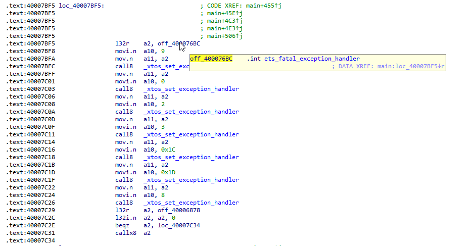
During boot, it sets up a series of exception handlers that point to a function that prints some information. However, these exceptions only provide partial information and are only available for certain types.
I have made various attempts to correctly implement the complete exception handlers, and it is possible, but not straightforward. The code that should be implemented is the same as the one already present in FreeRTOS:
- https://github.com/espressif/esp-idf/blob/ab03c2ea13ecaac1510b75e93b32cf0c472640fb/components/esp_system/port/panic_handler.c#L208
- https://github.com/espressif/esp-idf/blob/ab03c2ea13ecaac1510b75e93b32cf0c472640fb/components/esp_system/port/arch/xtensa/panic_handler_asm.S#L18
- https://github.com/espressif/esp-idf/blob/ab03c2ea13ecaac1510b75e93b32cf0c472640fb/components/xtensa/xtensa_context.S#L71
For this reason, I preferred to have the original bootloader that implements FreeRTOS and already has all the exception handlers implemented.
To generate the exception, we have different methods, the simplest one being to perform a write to a non writable area:
"movi a13, 0x93939393;"
"s32i.n  a2, a13, 0;"
This way, when necessary, with just one instruction, we will be able to see the complete context. Furthermore, using a unique method for all types of faults will allow us to perform a unified parsing in all situations and quickly identify if the injected glitch has allowed the instructions to continue until the end of the code.
Instructions to attack
The standard fault injection example uses loops or similar methods that do not allow us to understand in detail what is happening, thus it’s not an optimal approach. Instead, repeated instructions are arguably the best choice. However, in this case, we also want to understand precisely which ones we are affecting. By using a different increment value each time, we can understand which instruction we are influencing and what happens.
To determine which instruction we are affecting, we add a number that is equivalent to a single bit representation. This will speed up certain types of analysis:
"addi a6, a6, 0x1;"
"addi a6, a6, 0x2;"
"addi a6, a6, 0x4;"
"addi a6, a6, 0x8;"
"addi a6, a6, 0x10"
"addi a6, a6, 0x20"
"addi a6, a6, 0x40;"
The result of the operations will be as follows:
"addi a6, a6, 0x1;"  -> a6 = 0x01 (0b00000001)
"addi a6, a6, 0x2;"  -> a6 = 0x03 (0b00000011)
"addi a6, a6, 0x4;"  -> a6 = 0x07 (0b00000111)
"addi a6, a6, 0x8;"  -> a6 = 0x0F (0b00001111)
"addi a6, a6, 0x10"  -> a6 = 0x1F (0b00011111)
"addi a6, a6, 0x20"  -> a6 = 0x3F (0b00111111)
"addi a6, a6, 0x40;" -> a6 = 0x7F (0b01111111)
As a safety measure, we also check with IDA Pro that the code generated by the compiler is what we intended it to be:
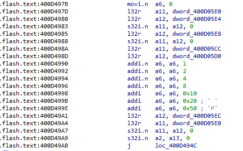
As we can see, probably due to some assembler optimizations, the code has been partially changed. In fact, the first instructions have been translated as “addi.n,” which are 16-bit instructions, instead of “addi,” which are 24-bit instructions. In terms of code functionality, the result remains unchanged, as the two instructions are equivalent.
By researching details in the “Xtensa Instruction Set Architecture (ISA) – Reference Manual,” we can find the following:
Assembler Note
The assembler may convert ADDI instructions to ADDI.N when the Code Density
Option is enabled and the immediate operand falls within the available range. If the immediate
is too large the assembler may substitute an equivalent sequence. Prefixing the
ADDI instruction with an underscore (_ADDI) disables these optimizations and forces
the assembler to generate the wide form of the instruction or an error instead.
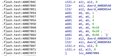
By modifying the assembly code as described at this point (replacing ADDI with _ADDI), we would get the “clean” code, which is also confirmed by the disassembling:
By conducting some tests, we found that approximately 12 instructions are executed in about 162ns. Considering that the compilation options set the frequency to 80Mhz and assuming that each instruction requires approximately 2 clock cycles, the timing looks reasonable:
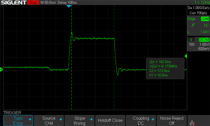
Using a frequency of 160Mhz, we have approximately 62 nanoseconds for the execution of 12 instructions:
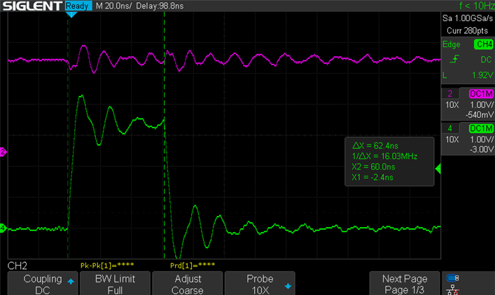
For convenience, let’s start working at 80Mhz to be more precise.
Putting everything together
To have a completely controlled environment, we need to perform the following steps:
- Set all registers to known values. This will help us understand what is happening.:
// a0 is return address, but not used anymore
"movi a0, 0x40404040;"

// a1 is the stack pointer (it's not a typo, I decided to exclude the a1 to have clean info into the stacktraces)
// "movi a0, 0x41414141;"

"movi a2, 0x42424242;"
"movi a3, 0x43434343;"
"movi a4, 0x44444444;"
"movi a5, 0x45454545;"
"movi a6, 0x46464646;"
"movi a7, 0x47474747;"
"movi a8, 0x48484848;"
"movi a9, 0x49494949;"
"movi a10, 0x50505050;"
"movi a11, 0x51515151;"
"movi a12, 0x52525252;"
"movi a13, 0x93939393;"
"movi a14, 0x54545454;"
"movi a15, 0x55555555;"
- Set the trigger:
// GPIO 26 PING HIGH using GPIO_OUT_W1TS
"movi a11, 0x4000000;"

"movi a12, 0x3ff44024;"
"s32i.n  a11, a12, 0;"

"movi a12, 0x3ff44008;"
"s32i.n  a11, a12, 0;"
- Modify the registers used during the trigger setup:
// Set correctly used registers
"movi a11, 0x51515151;"
"movi a12, 0x52525252;"
- Execute a series of NOPs to allow time for glitching and propagation:
// Execute NOP instructions
"nop;"
- Execute the code we want to attack:
"addi a6, a6, 0x1;"
"addi a6, a6, 0x2;"
"addi a6, a6, 0x4;"
"addi a6, a6, 0x8;"
"addi a6, a6, 0x10;"
"addi a6, a6, 0x20;"
"addi a6, a6, 0x40;"
- Execute a second series of NOPs to avoid glitching the final exception creation:
// Execute NOP instructions
"nop;"
- Set the trigger again to deactivate it:
// GPIO 26 PIN LOW using GPIO_OUT_W1TC
"movi a12, 0x3ff4400C;"
"movi a11, 0x4000000;"
"s32i.n  a11, a12, 0;"
- Generate a CPU exception:
// GENERATE CPU EXCEPTION
"s32i.n  a2, a13, 0;"
By running the entire code, we can observe that execution takes around a total of 25,200 nanoseconds:
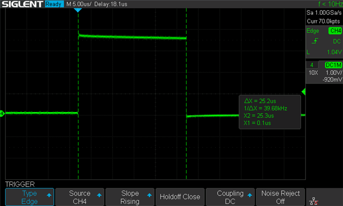
Glitching
Hardware setup
On the datasheet of the ESP32 processor, further details can be found on how the different VDD pins that provide power to the chip are used:
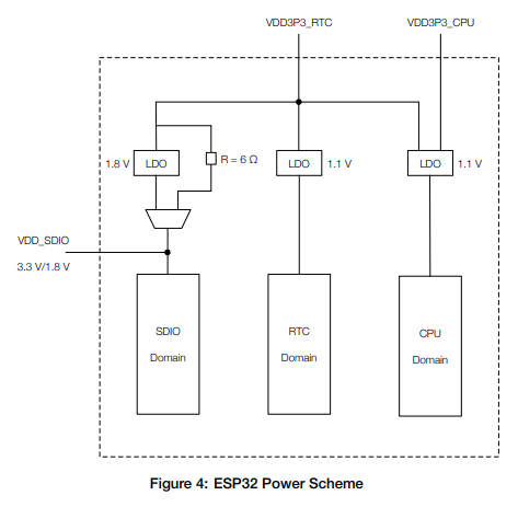
For this initial analysis, I decided to keep all VDD pins connected together, removing the capacitors connected to the VDD3P3_RTC and VDD3P3_CPU power lines.
The hardware on which the tests were performed has the following configuration, and the circled capacitors have been removed:
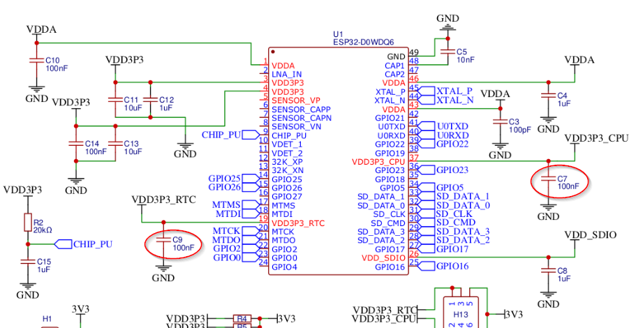
Source: https://github.com/raelize/TAoFI-Target/blob/main/files/schematic.png
Glitching preparation
Now that we have a “clean” environment just the way I like it, let’s look at the main features of the glitching script.
For convenience, we use the setup provided during the course, which includes:
- an ESP-PROG programmer with which we communicate via serial to the ESP32
- a Chipwhisperer Husky connected to the trigger PIN and responsible for performing crowbar glitching
- an RK6006 power supply to provide the ESP32 with a controlled voltage below the standard, making it more comfortable to execute faults; throughout all the tests, the power supply provides 2.13v to the ESP32 chip, which is below the threshold recommended by the manufacturer

After some initial tests, I have determined that the probable values for obtaining a good sample are as follows:
min_length = 400
max_length = 3000
min_delay = 4000
max_delay = 22000
To begin, we will use a “standard” configuration of the Husky:
cw_scope.clock.clkgen_src          = 'system'
cw_scope.clock.adc_mul             = 1
cw_scope.clock.clkgen_freq         = 200e6

# Glitching parameters
cw_scope.io.glitch_hp              = True
cw_scope.io.glitch_lp              = False
In the following articles of this series, we will also explore how we can make the most of the Husky.
However, the most important part is the initial classification that is performed before saving the result.
As we described earlier, we know that all the results should be “identical” because we use CPU exceptions that are all handled in the same way, whether our glitch is too long, causing an illegal instruction, or our glitch is too short and therefore does not affect code execution.
A specific routine is responsible for analyzing the result, comparing it with the expected result, and saving only the values that are “different” from the standard ones, in order to have a cleaner output during subsequent analysis.
A first interpretation of the results
With the “Glitch and pray” approach, we can start to see the first results and try to understand how to interpret them better. We have two varying values: the distance of the glitch from the trigger (delay) and the length of the performed glitch (length).
Some important assumptions:
- If PC is different from 0x400d713b (the address of the last instruction before the forged exception), we have not experienced a “clean” fault, so something broke beforehand. In the case of “illegal instruction” exceptions, it could help us understand which instruction caused the fault.
- If PC is equal to 0x400d713b (the address of the last instruction before the forged exception), we can interpret the results and understand which instructions we have influenced.
- All our target code works on the A6 registry; if A6 has not changed it is very likely that we have influenced instructions that are not of our interest.
All the results have been classified in this way:
- the green color represents “normal” results, the PC is correct and no modification of others registers has been detected
- the magenta color represents CPU restarts that usually happen if the glitch is too long
- the yellow color represents a fault with wrong PC, which means that we didn’t reach our final code
- the cyan color represents a fault where PC is correct (we reached our last instruction) and also A6 is correct, which means we didn’t fault our target instruction, but some other instruction
- the red color represents a fault where PC is correct (we reached our last instruction) and A6 doesn’t have the proper value, which means we faulted our target instruction
After 36K attempts, here are the first results:

The ones of interest to us are the red dots, where we have the correct PC but A6 doesn’t have the value we expected.
By cleaning up the results a little bit, we can see how the areas are quite concentrated:

We can find in blue some points of particular interest to us. For example, the “illegal instruction” in the first add operation. We can associate this behavior with “we have zeroed too many bits” of a specific instruction.
Searching for results Illegal.*PC: 0x400d70e4 we can identify parameters which lead us to corrupt our first target instruction which is at 0x400d70e4:

Looking for Illegal.*PC: 0x400d70e7 we can identify parameters which lead to corrupt the second instruction:

Looking for Illegal.*PC: 0x400d70ea we can identify parameters which lead to corrupt the third instruction:

Looking for Illegal.*PC: 0x400d70ed we can identify parameters which lead to corrupt the fourth instruction:

Looking for Illegal.*PC: 0x400d70f0 we can identify parameters which lead to corrupt the fourth instruction:

Looking for Illegal.*PC: 0x400d70f3 we can identify parameters which lead to corrupt the fifth instruction:

Looking for Illegal.*PC: 0x400d70f6 we can identify parameters which lead to corrupt the sixth instruction:

Executing some custom query on the data we can also find where we “skipped the instruction” (we will see later that this is not actually the case) by looking for the expected value in A6.
Looking for Store.* PC: 0x400d713b.*A6 : 0x0000007e we can identify parameters which lead to corrupt the first instruction in a way that the additional operation has not been executed:

Looking for Store.* PC: 0x400d713b.*A6 : 0x0000007d we can identify parameters which lead to corrupt the second instruction in a way that the additional operation has not been executed. In our initial test, no cases have been identified:

Looking for Store.* PC: 0x400d713b.*A6 : 0x0000007b we can identify parameters which lead to corrupt the third instruction in a way that the additional operation has not been executed:

Looking for Store.* PC: 0x400d713b.*A6 : 0x00000077 we can identify parameters which lead to corrupt the forth instruction in a way that the additional operation has not been executed:

Looking for Store.* PC: 0x400d713b.*A6 : 0x0000006f we can identify parameters which lead to corrupt the fifth instruction in a way that the additional operation has not been executed:

Looking for Store.* PC: 0x400d713b.*A6 : 0x0000005f we can identify parameters which lead to corrupt the sixth instruction in a way that the additional operation has not been executed:

Looking for Store.* PC: 0x400d713b.*A6 : 0x0000003f we can identify parameters which lead to corrupt the seventh instruction in a way that the additional operation has not been executed:

As we could see from the initial results, we can consider performing a very precise targeting of an instruction based on the time from the trigger.
However, the same results tell us that some instructions are more “simple” to target than others. I hypothesize that this is also due to the pipeline and internal caches of the processor.
A script to better understand the cause
One of the fundamental things taught in the course by @pulsoid and @tieknimmers is to debunk the myth of “an instruction was skipped”. Many who talk about glitching and fault injection wrongly use this term just to say “I didn’t understand what happened”.
To understand the results we are going to analyze, we need to hypothesize what will happen at the processor level. Since we are using the “crowbar to ground” technique, it is plausible to assume that during certain CPU operations (such as loading instructions, execution, memory copies, etc.), some bits which are 1 may turn into 0. Other techniques could yield different results, but this is the most likely effect in our situation.
To do this, I have developed a small script that, given a specific opcode, sets N bits to 0 and observes what the “corrupted” instruction would be. In an ideal world, fault injection could change a single bit, but currently we do not know if we can be that precise. Therefore, we must assume that we will change N different bits.
The script generates N different possibilities by assuming influence on N different bits. The bits that have changed from 1 to 0 are marked in red, while the bits that are among the selected N bits but have not changed because they were already set to 0 are marked in green. All possible variations that do not alter the instruction are ignored.
Let’s see, for example, what can happen to the instruction addi a6, a6, 0x1; in different scenarios assuming a variation from 1 to 4 bits.
Red bits are the ones changed, green bits are the ones that should been changed but already were set to 0.
The bit representation is consistent with that shown in the datasheet:
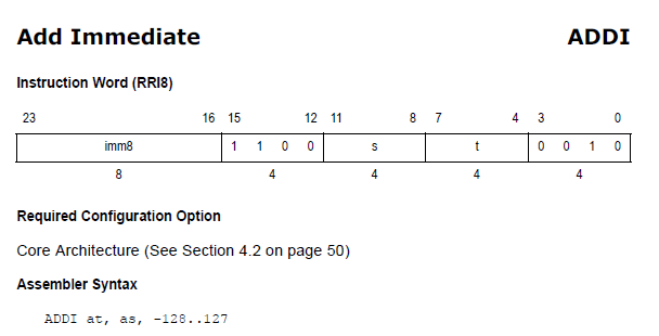
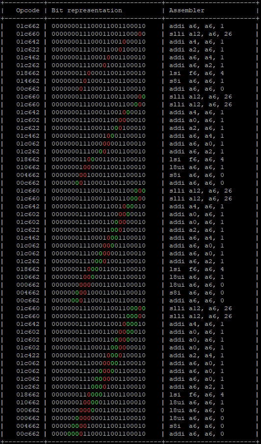
Alternatively, a “reduced” version that does not include duplicate cases:
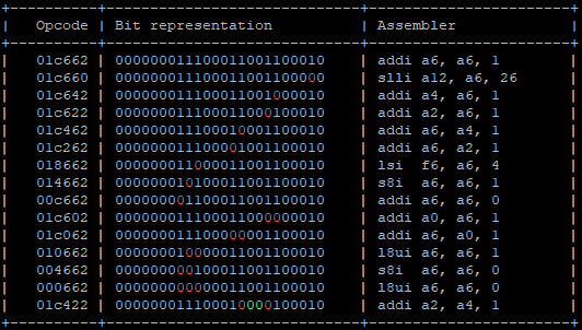
The code can be viewed at https://github.com/inode-/fault_injection/blob/main/OpcodeCalculator/opcode_calculator.py
A better interpretation of the results
Now let’s try to understand what actually happens at the processor level, assuming that “the instruction was skipped” is not a valid answer.
We start with the simplest cases and move towards the more complex and less “explainable” ones.
The results from a normal execution are as follows:
"addi a6, a6, 0x1;"  -> a6 = 0x01
"addi a6, a6, 0x2;"  -> a6 = 0x03
"addi a6, a6, 0x4;"  -> a6 = 0x07
"addi a6, a6, 0x8;"  -> a6 = 0x0F
"addi a6, a6, 0x10"  -> a6 = 0x1F
"addi a4, a6, 0x20"  -> a6 = 0x3F
"addi a6, a6, 0x40;" -> a6 = 0x7F
During the next steps, it is necessary to remember what the states of the registers are in a “normal” situation.
Core  0 register dump:
PC      : 0x400d713b  PS      : 0x00060430  A0      : 0x40404040  A1      : 0x3ffb4810
A2      : 0x42424242  A3      : 0x43434343  A4      : 0x44444444  A5      : 0x45454545
A6      : 0x0000007f  A7      : 0x47474747  A8      : 0x48484848  A9      : 0x49494949
A10     : 0x50505050  A11     : 0x04000000  A12     : 0x3ff4400c  A13     : 0x93939393
A14     : 0x54545454  A15     : 0x55555555  SAR     : 0x00000004  EXCCAUSE: 0x0000001d
EXCVADDR: 0x93939393  LBEG    : 0x400014fd  LEND    : 0x4000150d  LCOUNT  : 0xffffffff
Some typical examples are analyzed below. We have arbitrarily decided to consider that the maximum number of bits changed is 6, but the value could also be higher.
Level 1 (simple)
Difference between the normal registers:
StoreProhibited - PC: 0x400d713b - A6 : 0x00000077(0x0000007f) -
Which means:
- Expected value on A6 is 0x7F, we got 0x77 which means we have a difference of 0x8.
- Having a difference of 0x8 means that we faulted the 4th target instruction.
- No other registers have been affected.
- Calculating possible fault generated instructions, we can identify only one instruction which doesn’t generate a different CPU exception and causes the result to “add nothing”.
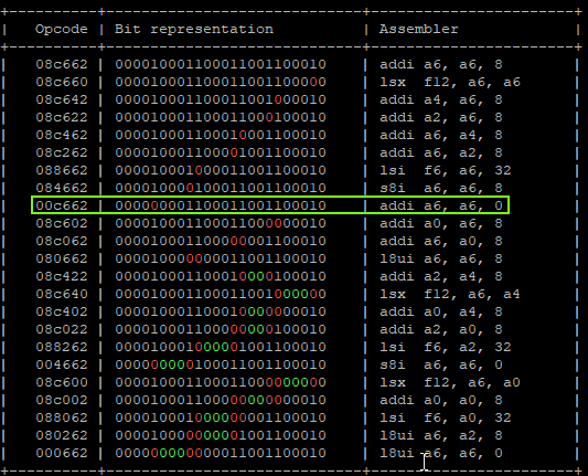
That will produce:
"addi a6, a6, 0x1;"  -> a6 = 0x01
"addi a6, a6, 0x2;"  -> a6 = 0x03
"addi a6, a6, 0x4;"  -> a6 = 0x07
"addi a6, a6, 0x0;"  -> a6 = 0x07 | GLITCHED
"addi a6, a6, 0x10"  -> a6 = 0x17
"addi a6, a6, 0x20"  -> a6 = 0x37
"addi a6, a6, 0x40;" -> a6 = 0x77
Level 2 (simple)
Difference between the normal registers:
StoreProhibited - PC: 0x400d713b - A4 : 0x0000003f(0x44444444) - A6 : 0x0000005f(0x0000007f) -
Which meanss:
- Expected value on A6 is 0x7F, we got 0x5f which means we have a difference of 0x20.
- Having a difference of 0x20 means that we faulted the 6th target instruction.
- Only register A4 has been changed, which means that in some way we have overwritten it.
- Calculating possible fault generated instructions, we can identify only one instruction which doesn’t generate a different CPU exception and causes the override of A4.
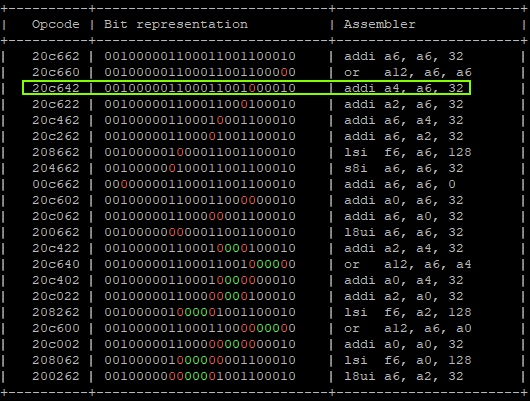
That will produce:
"addi a6, a6, 0x1;"  -> a6 = 0x01
"addi a6, a6, 0x2;"  -> a6 = 0x03
"addi a6, a6, 0x4;"  -> a6 = 0x07
"addi a6, a6, 0x8;"  -> a6 = 0x0F
"addi a6, a6, 0x10"  -> a6 = 0x1F
"addi a4, a6, 0x20"  -> a6 = 0x1F, a4 = 0x3F | GLITCHED
"addi a6, a6, 0x40;" -> a6 = 0x5F, a4 = 0x3F
Level 3 (simple)
StoreProhibited - PC: 0x400d713b - A2 : 0x40404041(0x42424242) - A6 : 0x0000007e(0x0000007f) -
Which means:
- Expected value on A6 is 0x7F, we got 0x7e which means we have a difference of 0x1.
- Having a difference of 0x1 means that we faulted the 1st target instruction.
- Register A2 contains the value of A0 plus one, which means that we changed both source and destination register in a single fault.
- Calculating possible fault generated instructions, we can identify only one instruction which doesn’t generate a different CPU exception and causes the override of A2 using A0 as source.
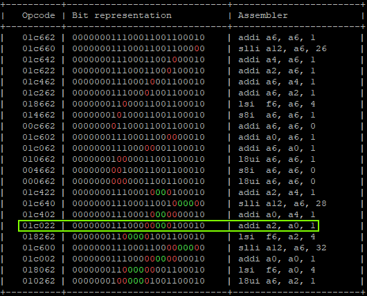
That will produce:
"addi a6, a6, 0x1;"  -> a6 = 0x00, a2 = 0x40404041 | GLITCHED
"addi a6, a6, 0x2;"  -> a6 = 0x02, a2 = 0x40404041
"addi a4, a6, 0x4;"  -> a6 = 0x06, a2 = 0x40404041
"addi a6, a6, 0x8;"  -> a6 = 0x0E, a2 = 0x40404041
"addi a6, a6, 0x10"  -> a6 = 0x1E, a2 = 0x40404041
"addi a6, a6, 0x20"  -> a6 = 0x3E, a2 = 0x40404041
"addi a6, a6, 0x40;" -> a6 = 0x7E, a2 = 0x40404041
Level 4 (simple)
StoreProhibited - PC: 0x400d713b - A4 : 0x00000007(0x44444444) - A6 : 0x0000007b(0x0000007f) -
Which means:
- Expected value on A6 is 0x7F, we got 0x7b which means we have a difference of 0x4.
- Having a difference of 0x4 means that we faulted the 3rd target instruction.
- Only register A4 has been changed, which means that in some way we have overwritten it.
- Calculating possible fault generated instructions, we can identify only one instruction which doesn’t generate a different CPU exception and causes the override of A4.
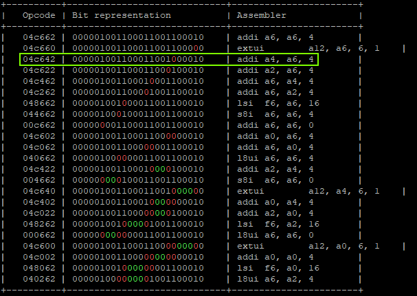
That will produce:
"addi a6, a6, 0x1;"  -> a6 = 0x01
"addi a6, a6, 0x2;"  -> a6 = 0x03
"addi a4, a6, 0x4;"  -> a6 = 0x03, a4 = 0x7 | GLITCHED
"addi a6, a6, 0x8;"  -> a6 = 0x0B, a4 = 0x7
"addi a6, a6, 0x10"  -> a6 = 0x1B, a4 = 0x7
"addi a6, a6, 0x20"  -> a6 = 0x3B, a4 = 0x7
"addi a6, a6, 0x40;" -> a6 = 0x7B, a4 = 0x7
Level 5 (medium)
StoreProhibited - PC: 0x400d713b - A0 : 0x0000001f(0x40404040) - A4 : 0x0000002f(0x44444444) - A6 : 0x0000004f(0x0000007f) -
Which means:
- Expected value on A6 is 0x7F, we got 0x4f which means we have a difference of 0x30.
- Having a difference of 0x30 means that we faulted 2 target instructions, the 6th and the 7th.
- The A0 register contains the exact result of the standard 6th instruction.
- The A4 register contains a fault compatible with “the skip” of the 6th instruction and the sum generated from the 7th instruction.
- Calculating possible fault generated instructions, we can identify only one instruction which doesn’t generate a different CPU exception and causes the override of A0 and A4 in the correct way.
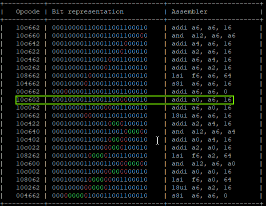
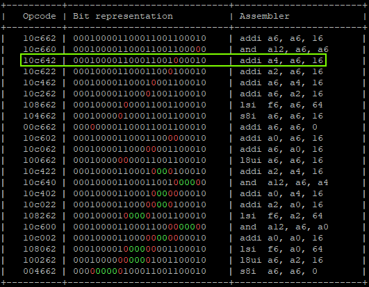
That will produce:
"addi a6, a6, 0x1;"  -> a6 = 0x01
"addi a6, a6, 0x2;"  -> a6 = 0x03
"addi a6, a6, 0x4;"  -> a6 = 0x07
"addi a6, a6, 0x8;"  -> a6 = 0x0F
"addi a0, a6, 0x10"  -> a6 = 0x0F, a0 = 0x1F             | GLITCHED
"addi a4, a6, 0x20"  -> a6 = 0x0F, a0 = 0x1F, a4 = 0x2F  | GLITCHED
"addi a6, a6, 0x40;" -> a6 = 0x7F
Level 6 (medium)
StoreProhibited - PC: 0x400d713b - A4 : 0x00000005(0x44444444) - A6 : 0x00000079(0x0000007f) -
Which means:
- Expected value on A6 is 0x7F, we got 0x79 which means we have a difference of 0x6.
- Having a difference of 0x6 means that we faulted 2 target instructions, the 2nd and the 3rd.
- The A4 register contains a value that is compatible if the second instruction has not modified A6.
- Calculating possible fault generated instructions, we can identify only two instructions which don’t generate a different CPU exception and cause the override of A4 in the correct way.
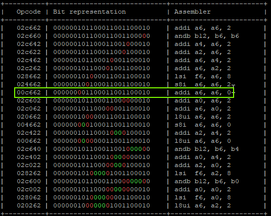
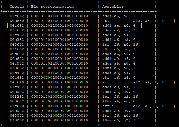
That will produce:
"addi a6, a6, 0x1;"  -> a6 = 0x01
"addi a6, a6, 0x0;"  -> a6 = 0x01              | GLITCHED
"addi a4, a6, 0x4;"  -> a6 = 0x01, a4 =  0x5   | GLITCHED
"addi a6, a6, 0x8;"  -> a6 = 0x09, a4 =  0x5
"addi a6, a6, 0x10"  -> a6 = 0x19, a4 =  0x5
"addi a4, a6, 0x20"  -> a6 = 0x39, a4 =  0x5
"addi a6, a6, 0x40;" -> a6 = 0x79, a4 =  0x5
Level 7 (medium)
StoreProhibited - PC: 0x400d713b - A6 : 0x42424262(0x0000007f) -
Which means:
- The A6 register has been modified with the content of A2 (0x42424242).
- Difference between A2 and final A6 is 0x42424262 – 0x42424242 which is 0x20 meaning that we faulted the 6th target instruction.
- Register A6 is missing 0x40 which is the add of the last target instruction, so we corrupted 2 instructions.
- Calculating possible fault generated instructions, we can identify only one instruction which doesn’t generate a different CPU exception and causes the override of A6 with A2 value (6th instruction).
- Calculating possible fault generated instructions, we can identify one instruction which potentially doesn’t generate a different CPU exception and does nothing on A6.
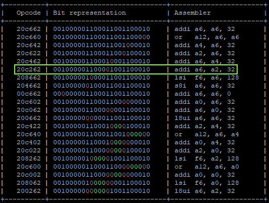
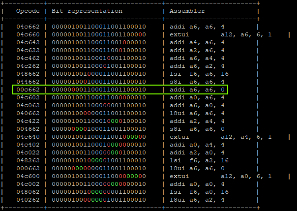
That will produce:
"addi a6, a6, 0x1;"  -> a6 = 0x01
"addi a6, a6, 0x2;"  -> a6 = 0x03
"addi a6, a6, 0x4;"  -> a6 = 0x07
"addi a6, a6, 0x8;"  -> a6 = 0x0F
"addi a6, a6, 0x10"  -> a6 = 0x1F
"addi a6, a2, 0x20"  -> a6 = 0x42424262 | GLITCHED
"addi a6, a6, 0x00"  -> a6 = 0x42424262 | GLITCHED
Interpretation of the results – another approach
Comparing the possible instructions on which we have made a fault is possible in simple cases. However, in more complex scenarios it becomes difficult to manually explain the cases. For this reason, I have decided to also take another path, to emulate the execution of the fault in a virtual environment and subsequently compare the result. My first choice would have been to use Unicorn Engine, but unfortunately it does not currently support the XTENSA CPU.
Another feasible approach could have been to use the JTAG port combined with GDB to modify the instructions and the context, to execute the instructions step by step and see what had changed. Technically feasible but probably too slow to perform as many emulations as we need.
We then decided to try the emulation feature of Ghidra, which is poorly documented but should be supported for all CPUs. In fact, unlike for example IDA Pro, practically all processors come with what is defined as “P-Code”, that is, what a certain assembler operation performs. The P-Code abstraction is also what allows Ghidra to perform decompilation on almost all supported processors.
Ghidra CPU emulation
Some examples of using Ghidra for instruction emulation that I’ve used as a starting point:
- https://gist.github.com/cetfor/18cae544249e4cf78f66930175072876
- https://medium.com/@cetfor/emulating-ghidras-pcode-why-how-dd736d22dfb
Reusing part of the Python code presented earlier, I decided to export the possible instructions that could be executed and import them directly into the code of our plugin.
At this point, as a first step, we must modify the binary to reflect the instructions we want to emulate:
void patch_code(long newcode[]) throws CancelledException, MemoryAccessException
{
	Address current_instruction = currentProgram.getAddressFactory().getDefaultAddressSpace().getAddress(init_addr);

	for(int i = 0; i < newcode.length; i++)
	{
		clearListing(current_instruction);

		this.setBytes(current_instruction, longToBytes_24bits(newcode[i]));
		current_instruction = current_instruction.add(3);
	}

	disassemble(currentProgram.getAddressFactory().getDefaultAddressSpace().getAddress(init_addr));
	return;

}
Then we set the context exactly as what is expected by the CPU:
emuHelper.writeRegister("a0", 0x40404040);
emuHelper.writeRegister("a1", 0x41414141);
emuHelper.writeRegister("a2", 0x42424242);
emuHelper.writeRegister("a3", 0x43434343);
emuHelper.writeRegister("a4", 0x44444444);
emuHelper.writeRegister("a5", 0x45454545);
emuHelper.writeRegister("a6", 0x46464646);
emuHelper.writeRegister("a7", 0x47474747);
emuHelper.writeRegister("a8", 0x48484848);
emuHelper.writeRegister("a9", 0x49494949);
emuHelper.writeRegister("a10", 0x50505050);
emuHelper.writeRegister("a11", 0x51515151);
emuHelper.writeRegister("a12", 0x52525252);
emuHelper.writeRegister("a13", 0x93939393);
emuHelper.writeRegister("a14", 0x54545454);
emuHelper.writeRegister("a15", 0x55555555);

emuHelper.writeRegister("a6", 0x0);
Afterwards, we execute the instructions of interest:
	emuHelper.writeRegister(emuHelper.getPCRegister(), initial_instruction);

	int j = 0;

	for(int i = 0; i<=array_size; i++)
	{
		Address executionAddress = emuHelper.getExecutionAddress();

		outfile.write(executionAddress.toString() + ' ' + getInstructionAt(executionAddress) + "\n");

		try {
			boolean success = emuHelper.step(monitor);

			j++;
			if( success == false) {
				String lastError = emuHelper.getLastError();
				outfile.write(lastError  + " - " +  getInstructionAt(executionAddress) + "\n");
				outfile.write(HexFormat.of().formatHex(getBytes(executionAddress, 3)));
				return -1;
			}
		} catch (Exception e) {
			println(e.toString());
			return -1;

		}

	}
At this point, we compare the results and save only those that are different from what we expect:
		if(emuHelper.readRegister("a0").longValue() != 0x40404040 )
			outfile.write("A0 : 0x" + String.format("%08x", emuHelper.readRegister("a0").longValue()) + " ");
		if(emuHelper.readRegister("a1").longValue() != 0x41414141 )
			outfile.write("A1 : 0x" + String.format("%08x",emuHelper.readRegister("a1").longValue()) + " ");
		if(emuHelper.readRegister("a2").longValue() != 0x42424242 )
			outfile.write("A2 : 0x" + String.format("%08x",emuHelper.readRegister("a2").longValue()) + " ");
		if(emuHelper.readRegister("a3").longValue() != 0x43434343 )
			outfile.write("A3 : 0x" + String.format("%08x",emuHelper.readRegister("a3").longValue()) + " ");
		if(emuHelper.readRegister("a4").longValue() != 0x44444444 )
			outfile.write("A4 : 0x" + String.format("%08x",emuHelper.readRegister("a4").longValue()) + " ");
		if(emuHelper.readRegister("a5").longValue() != 0x45454545 )
			outfile.write("A5 : 0x" + String.format("%08x",emuHelper.readRegister("a5").longValue()) + " ");
		if(emuHelper.readRegister("a6").longValue() != 0x7f )
			outfile.write("A6 : 0x" + String.format("%08x",emuHelper.readRegister("a6").longValue()) + " ");
		if(emuHelper.readRegister("a7").longValue() != 0x47474747 )
			outfile.write("A7 : 0x" + String.format("%08x",emuHelper.readRegister("a7").longValue()) + " ");
		if(emuHelper.readRegister("a8").longValue() != 0x48484848 )
			outfile.write("A8 : 0x" + String.format("%08x",emuHelper.readRegister("a8").longValue()) + " ");
		if(emuHelper.readRegister("a9").longValue() != 0x49494949 )
			outfile.write("A9 : 0x" + String.format("%08x",emuHelper.readRegister("a9").longValue()) + " ");
		if(emuHelper.readRegister("a10").longValue() != 0x50505050 )
			outfile.write("A10 : 0x" + String.format("%08x",emuHelper.readRegister("a10").longValue()) + " ");
		if(emuHelper.readRegister("a11").longValue() != 0x51515151 )
			outfile.write("A11 : 0x" + String.format("%08x",emuHelper.readRegister("a11").longValue()) + " ");
		if(emuHelper.readRegister("a12").longValue() != 0x52525252 )
			outfile.write("A12 : 0x" + String.format("%08x",emuHelper.readRegister("a12").longValue()) + " ");
		if(emuHelper.readRegister("a13").longValue() != 0x93939393L )
			outfile.write("A13 : 0x" + String.format("%08x",emuHelper.readRegister("a13").longValue()) + " ");
		if(emuHelper.readRegister("a14").longValue() != 0x54545454 )
			outfile.write("A14 : 0x" + String.format("%08x",emuHelper.readRegister("a14").longValue()) + " ");
		if(emuHelper.readRegister("a15").longValue() != 0x55555555 )
			outfile.write("A15 : 0x" + String.format("%08x",emuHelper.readRegister("a15").longValue()) + " ");
		outfile.write(HexFormat.of().formatHex(getBytes(currentProgram.getAddressFactory().getDefaultAddressSpace().getAddress(init_addr), 3*7)));
		outfile.write("\n");
Full code available at https://github.com/inode-/fault_injection/blob/main/GhidraEmulation/xtensa_emulator.java
Pros and cons
One of the main pros of this approach is the possibility of having an emulator up and running in a very short time, even though Ghidra’s APIs are poorly documented. However, there are also a number of cons:
- the procedure to emulate everything is slow
- we cannot be certain that some exceptions are handled in the same way by the emulation layer as by the original hardware
Conclusions
One thing we can state with certainty is that instructions are not “skipped”…
Sometimes it is not easy to explain what happens in the context of fault injection, but it is possible to try to understand what happened if there is a clear context. Of course, we cannot be certain, but we can come to have a good degree of confidence in understanding what happened in some cases. In the next articles in this series, I will try to find other ways to interpret the results.
Another important finding is that somehow it is possible to affect multiple instructions, and the modified bits don’t have to be contiguous.
Certainly, this article does not intend to be exhaustive, and I know there are many opportunities for improvement. For example, in the context we are working on, the floating-point registers are not printed, but as a start, I would dare to say that it is more than enough.
Once again, I’d like to thank @tieknimmers and @pulsoid for their invaluable support during the writing of this article and for putting up with my endless questions and queries.